As of yesterday (19 Sept 2016) DLS has its first set of playable levels! 37 to be exact :)
Level types
Currently there are 3 different level types. Combinational circuits, sequential circuits and stream processing circuits.
Combinational circuits
In a combinational circuit level your goal is to build a circuit which, given some specific inputs, will produce the expected outputs combinationally i.e. will react to input changes immediately, without the use of flip flops, registers and clocks. Figure 1 shows such a level.
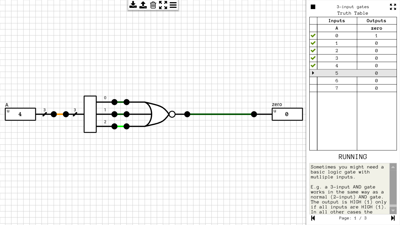
On the right side of the screen it’s the truth table you are expected to match. The input and output values might be random, depending on the level. E.g. if the inputs are narrow enough to be able to exhaust all possible input values, then the truth table is hardcoded and will never change. Otherwise, the inputs are randomized every time you start the level.
Since there’s no clock involved in these levels, the only property you might want to optimize is the total number of transistors used to create the circuit. More details on this below.
Sequential circuits
In this type of level, your goal is to build a circuit which will produce the expected output at specific simulation timesteps. Figure 2 shows such a level.
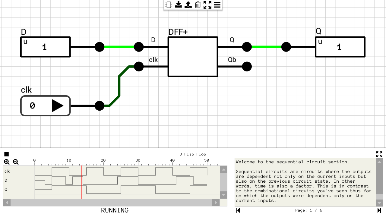
The timing graph at the bottom of the screen shows the clock, the input values at specific timesteps and the expected outputs.
Side note: There are two different timelines in DLS: the steady state timeline and the transient (or internal) timeline. Given an initial steady state of a circuit, every change to an input value generates an event at time 0 of the internal timeline. Depending on the type of gates this input is connected to, new events are generated at future internal timesteps, based on the gate’s propagation delay. This cycle of event generation and propagation is repeated until no more new events are generated. At this point the circuit has reached a new steady state and the steady state timeline is advanced. The timing graph in all sequential levels corresponds to the steady state timeline. It doesn’t matter how long it took the result to be calculated, in terms of internal timesteps/gate delays, as long as the circuit reaches a new steady state.
In contrast to the combinational levels, these levels include a clock, but since its value over time is hardcoded, the only property you might want to optimize is the total number of transistors used to create the circuit.
Stream processing circuits
The last type of level is, in my opinion, the most interesting. You get as input a stream of data and a clock. Your goal is to create a circuit which will read the input stream(s) and generate the expected output stream(s). In this case, each input stream has its own load signal and each output stream has its own write signal. Every time a rising edge is detected on one of those, a new value is loaded or written from/to the corresponding port. Figure 3 shows one such level.
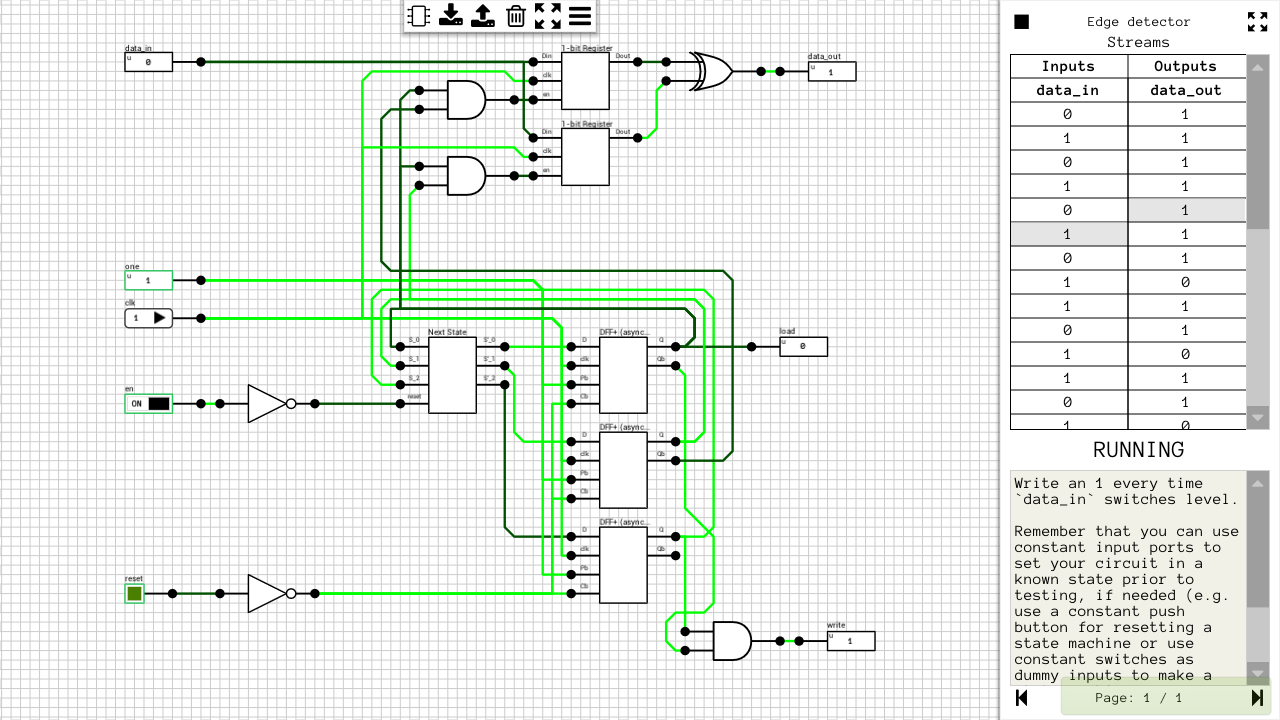
You can implement those circuits in any way you want. This time, the clock is continuously ticking, but since you load and write data at your own pace, one extra property you might want to optimize for is the total number of clock ticks it takes for your circuit to process all the data. E.g. if you are able to produce 2 or more values in the same clock tick, you only have to produce 2 rising edges on the corresponding write output. The same is true for loading the input streams.
Transistor Count and Maximum Clock Frequency
I wanted to add some form of scoring mechanism to all the levels and the total number of transistors used in the circuits is the most common one I could use. The number of transistors for each build-in gate is supposed to be based on a CMOS implementation. E.g. a 2-input NAND/NOR gate requires 4 transistors, an inverter gate requires 2 transistors and a 2-input AND/OR gate requires 6 transistors (4 for the NAND/NOR + 2 for the inverter).
Another way of measuring the efficiency of a circuit is to calculate the delay of its critical path. Knowing the critical path delay, we can estimate the maximum clock frequency a circuit can operate with.
Unfortunately, calculating the critical path of an arbitrary circuit isn’t that simple. As far as I know, all the algorithms used for such a task by logic simulators use a dedicated flip flop component in order to be able to break a sequential circuit into combinational parts and sync points. Knowing that kind of info, one can calculate the critical path of each combinational part. The slowest part is the own which indicates the maximum operating clock frequency.
Since DLS doesn’t have such a dedicated flip flop component, this is nearly impossible to implement. The only way I can estimate the critical path delay of an arbitrary circuit in DLS is by repeatedly simulating the circuit with random inputs and calculating the total internal timesteps it took to produce the outputs. The problem is that in order to reliably estimate the critical path delay this way requires too many simulations, which in turn require extra time.
The advantage of this kind of measurement is that techniques such as pipelining will show their benefit by allowing faster clocks to be used. I’ll reconsider it for a future version.
That’s all for now. Hope to find some more time to work on new levels and different level types. Until then, you can send your feedback on Twitter.