A couple of days ago I started playing with Emscripten to see if DLS can run in the browser. Apparently it can!
So, I decided to remove the obselete v0.10.1 I was keeping as a demo, since the differences between that and the latest version (0.14) are big.
You can evaluate DLS’ capabilities with the online sandbox from now on. I added a link to it to the Links section on the game’s page on itch.io. In case you decide to purchase DLS in order to run it on your desktop (and/or support further development) and it doesn’t work correctly (i.e. due to an untested Linux distro), I’ll be glad to hear about it and try to fix it.
Finally, note that even though the online sandbox supports all the features of the desktop version, there are no puzzles and the performance isn’t on par with the desktop version (if your browser supports it, I’d recommend running the WebAssembly version).
TL;DR: New version is out; further development is paused for now (only bug fixes and small improvements); making games is hard and it’s really easy to loose focus if you don’t have a plan :)
Two days ago I uploaded v0.14 of DLS on itch.io and GameJolt. This will probably be the last update for a long time, at least in its current form. The reason for this is because I need to figure out where I’m going to take DLS from here.
Before writing anything else, I’d like to thank everyone who took the time to download and play with it, especially those who submitted feedback and those who spent their money on it.
My initial goal was to write a simple logic simulator and then build some kind of game around it (preferably interesting and fun :)). Unfortunately, I didn’t have a concrete plan on the game part from the beginning, so I ended up focusing on the simulator most of the time. The end result is a simulator capable enough to simulate a real CPU, although it’s microcoded (i.e. most of the instruction decoding is implemented using ROMs instead of logic gates) and the simulation speed isn’t really great (only 1.3ms/sec with a 20MHz clock). By the way, I was planning on writing at least one blog post on it but I haven’t found the time yet.
As you probably know, DLS already includes some puzzles for you to solve. The problem with those (as I see it) is that they are either too simple or too complicated. Taking into account the fact that there’s no physical, real world, meaning to the objectives of each level, makes them even more complex. I.e. there’s a sequential level which requires the player to build a 4-bit Serial-in/Parallel-out circuit. In my opinion, it would be more interesting if the output of the circuit was some kind of ASCII message reconstruction shown on an LCD display. The objective of the puzzle would stay (more or less) the same, but the output would have been a bit more interesting.
It’s things like that that really bother me with the current state of the game and I need some time to think about them and decide how to move forward. As far as I can tell, there are 3 different ways to go.
Abandon the game idea completely and focus on the sandbox/simulator.
Keep the same kinds of puzzles and try to make them better and more interesting.
Create a completely different kind of game which will use the simulator as the primary way of achieving certain goals.
Ultimately, I’d like to build no. 3 but I don’t know where to begin and what the bigger picture will be.
No. 1 isn’t much of an option because (as I’ve written in a previous post) I’m not qualified enough to build a better logic simulator. There are many different kinds of logic simulators out there which do things faster and better than DLS. If I decide to take this route there are a lot of things to change and add, and the final product will probably won’t have many things in common with the current version.
No. 2 seems like the best option right now, because I already have the base for it. But in its current state it’s missing the “interesting and fun” part I mentioned earlier.
Having said the above, I will continue working on it in my spare time. I’ll be fixing bugs and trying to make the UI more functional and easier to use. And more importantly, I’ll continue to take notes based on your feedback, hoping that it’ll push me to the right direction :)
Thanks for reading!
PS. Here’s a list of games to keep you busy in the meantime (WARNING: I have no connection with those games or their developers and I haven’t played most of them)
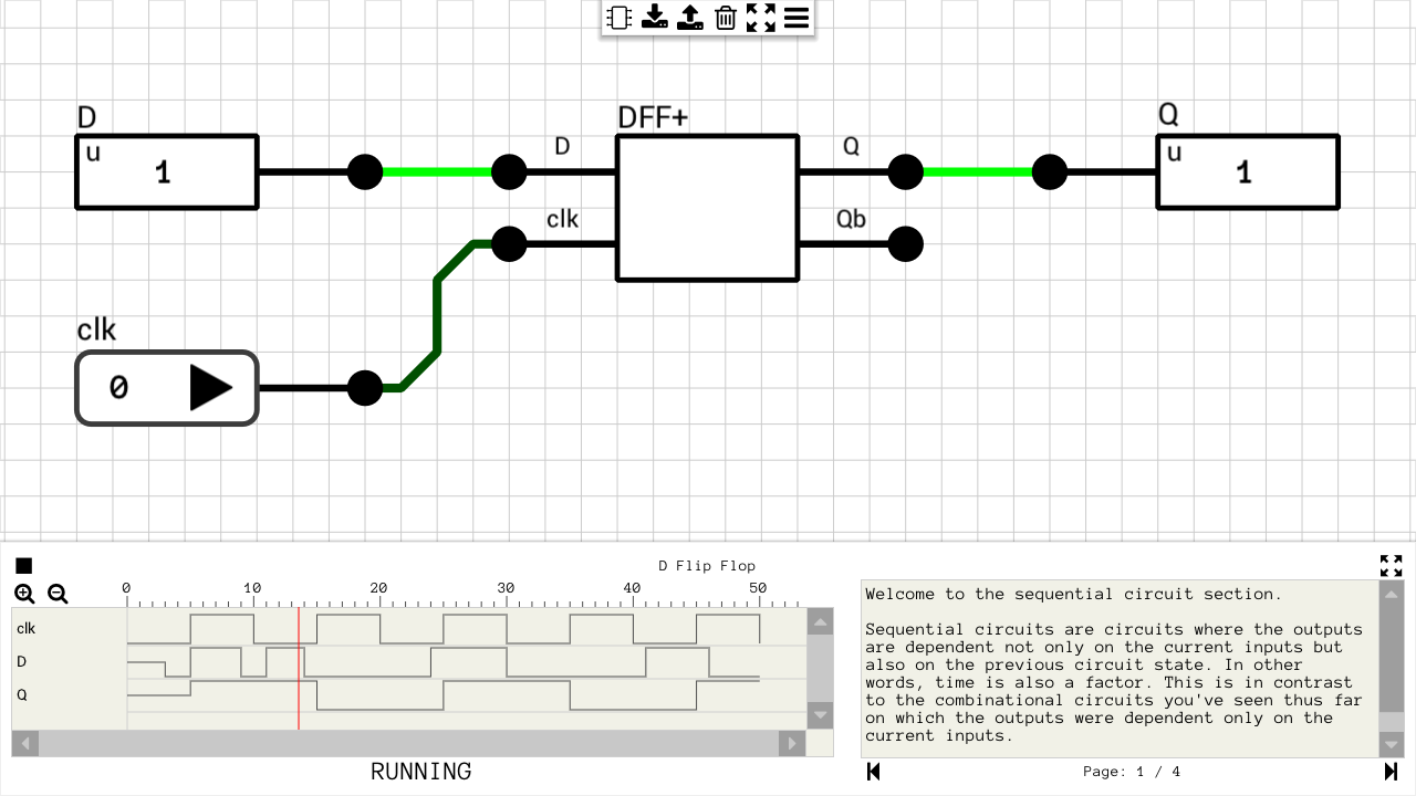
If you ever tried to create a counter in a logic simulator, chances are that you have created a state machine using the build-in flip flop components offered by the simulator (most of them have dedicated components for D-type or JK flip flops).
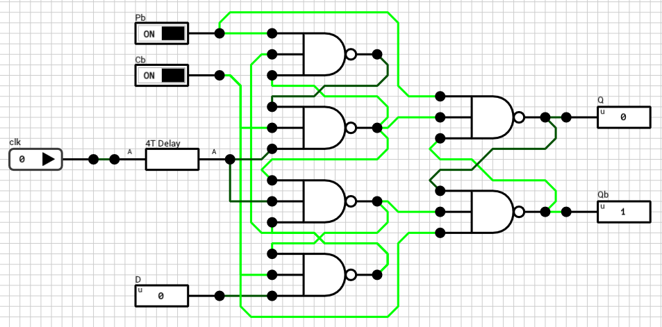
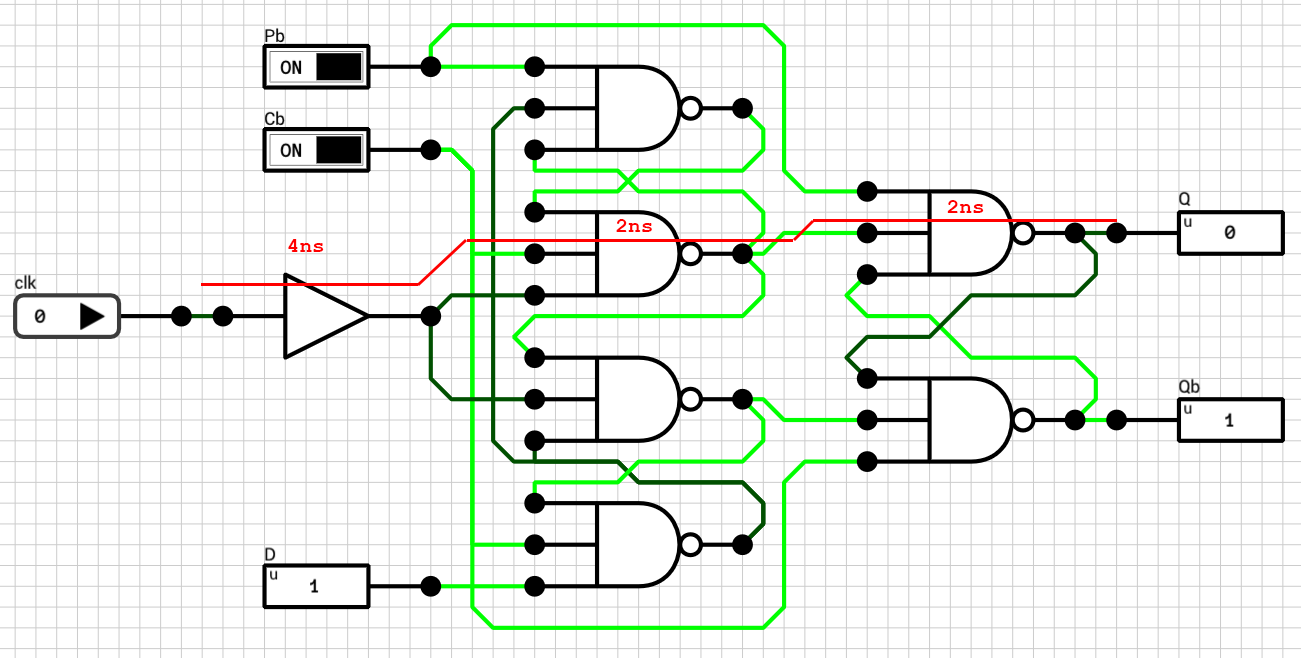
In DLS there’s no such component. You have to create your own flip flop, out of basic logic gates, and use it to build your counter. Figure 1 shows the positive edge triggered D flip flop I used in previous posts to create the register file.
Figure 1: Positive-edge-triggered D flip-flop used in the Register File circuit
In most cases, building a counter using this FF will work fine. E.g. if the counter’s output is used as an input to a combinational network with its output value connected to another FF, which will in turn be latched at the next clock tick.
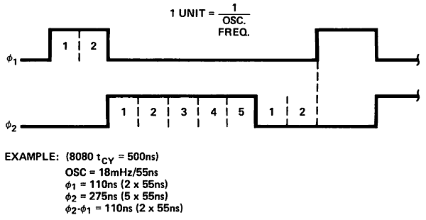
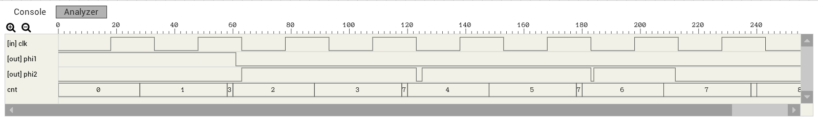
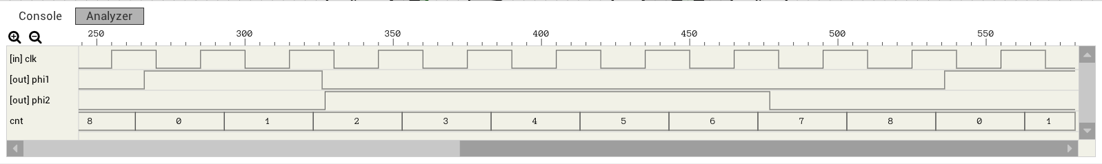
But there’s another use for a counter. You can use a counter to build specific sequences of pulses, such as the two phase clock shown in figure 2. This is the theoretical output of an
i8224. Phase 1 (phi1) is HIGH for 2 clock ticks. It then goes to LOW and phase 2 (phi2) goes to HIGH for the next 5 clock ticks. After that, both phases are LOW for 2 extra ticks.
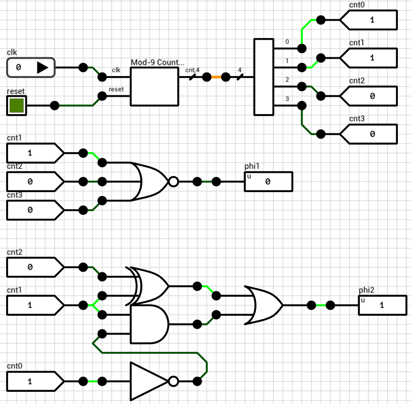
In order to build such clock, we can use a mod-9 counter (since there are 9 ticks in a cycle). A mod-9 counter counts from 0 to 8 and then wraps around. Figure 3 shows the schematic of the counter. Note that since the maximum value of 8 requires 4 bits, there are 4 flip flops in the schematic.
Figure 3: Mod-9 counter
Figure 4 below shows the two phase clock circuit using the mod-9 counter. Phase 1 is HIGH when cnt is 0 or 1. Otherwise it’s LOW. Phase 2 is HIGH when cnt is 2, 3, 4, 5 or 6, otherwise it’s low. The two outputs, phi1 and phi2 are used as clock inputs to an i8080 CPU.
Figure 4: 2-phase clock generator
Theoretically, everything should work correctly if we use the FF from figure 1. The counter should count from 0 to 8, phi1 and phi2 will be calculated based on the counter’s value and the i8080 should function as expected. Unfortunately, this isn’t the case (otherwise I wouldn’t have written this :)). Let’s take a look at the timing output of the circuit from figure 4, where the mod-9 counter has been implemented using the FF from figure 1.
Figure 5: Wrong 2-phase clock timing graph
phi1 looks correct. But phi2 has 2ns spikes every time the next counter value requires 2 bits to be flipped (e.g. from 1 to 2, bit #0 should go from HIGH to LOW and bit #1 should go from LOW to HIGH). This is because the FF from figure 1 has a different clk-to-Q propagation delay depending on whether Q is going to rise (0 to 1) or fall (1 to 0). Figures 6 and 7 show the critical path for both cases.
Figure 6: D FF critical path for LOW to HIGH transitionFigure 7: D FF critical path for HIGH to LOW transition
When Q is going to rise, the rising edge of the clk requires 8ns to reach it. When Q is going to fall, the clk signal requires 10ns to reach it. There is a 2ns difference between the two cases and this is the reason for the spikes in figure 5. The mod-9 counter generates the sequence 0, 1, 3, 2, 3, 7, 4, 5, etc., instead of the expected sequence of 0, 1, 2, 3, 4, 5, etc., because bits go from LOW to HIGH faster than they go from HIGH to LOW.
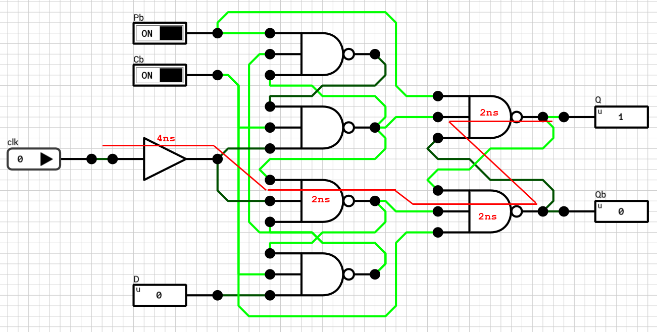
The fix is easy given the paths from figures 6 and 7. The best we can do is to make the fast path a bit slower. This can be achieved by inserting a 2ns buffer as shown in figure 8.
Figure 8: Positive-edge-triggered D flip-flop with equal rising and falling propagation delays
Figure 9 shows the timing graph of the two phase clock using a mod-9 counter implemented with the FF from figure 8.
Figure 9: Correct 2-phase clock timing graph
Note: The final FF from figure 8 still includes the 4ns buffer after the clk which I added in a previous post for the register file. This buffer is used to synchronize clk and D in case both of them switch at the same time. In other words, it makes the setup time of the FF equal to 0 (tS = 0). In the counter case, this delay shouldn’t be needed. By removing the buffer, the FF’s propagation delay can be reduced to 6ns instead of 10ns. This means that the counter can work with a faster clock.
Thanks for reading. Comments/suggestions/corrections are
welcome.
If you happen to be one of the two readers of this blog who have actually checked out the circuits I’ve posted, you might have found out that the register file circuit (RF) I presented in an
earlier post doesn’t work quite right. If you tried it out by manually changing the input values (e.g. rD and dD), everything appears to work correctly. Whenever the clock ticks, the new value is written to the selected register.
The problem I’m going to talk about appears when you try to use this component as part of a larger circuit. If you connect your clock directly to the clk input of the RF but the dD and rD inputs are connected to some other component’s output, you’ll need 2 clock ticks to actually write the new value to the selected register. This is because I didn’t pay attention to propagation delays when designing the various components and the clock signal arrives to the flip flops before the new data signal.
So, let’s fix the circuit by starting from the basic element of the RF, as I did in the original post.
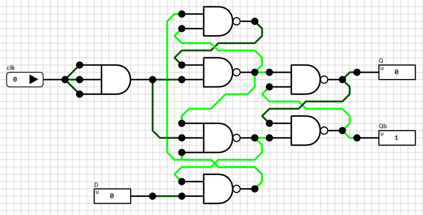
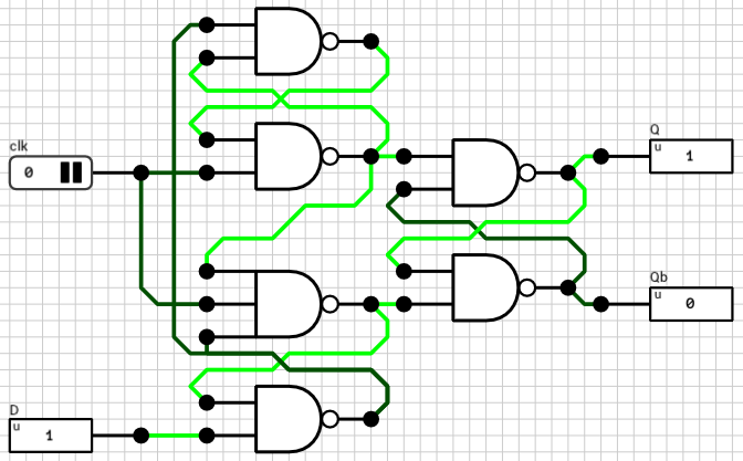
Positive edge triggered D flip flop
The original DFF I used is shown in figure 1 for reference. Ideally, whenever clk goes from LOW to HIGH, the current D value is reflected on the Q output. Unfortunately, this isn’t true. In order to test it out we need a testbench. Since D is an 1-bit signal, there are two transitions to consider: D going from LOW to HIGH and vice versa.
Figure 1: The original Positive Edge Triggered D Flip Flop circuit
There are 3 different cases when it comes to the timings of clk and D inputs.
clk signal arrives before D
clk signal arrives at the same time as D
clk signal arrives after D
Cases 2 and 3 are the ones we are interested in. The 1st case works correctly because if the clock signal arrives before the new data, it means that the controlling circuit wanted to write the old data to the flip flop. In other words, it’s the controlling circuit’s responsibility to synchronize the two signals.
On the other hand, if the rising edge of clk arrives after the new D value, we must assume that the new data will be written to the flip flop. So, the worst case scenario is that both clk and D arrive at the exact same time.
In order to find out if the current circuit works as expected, I used a testbench. Testbenches are an easy way to change multiple input values at the same time before triggering a simulation. Script 1 below shows the testbench I used.
-- Reset the circuit to a known state
set("clk", 0);
set("D", 0);
simulate();

-- D 0 -> 1
set("D", 1);
tick("clk");
assert(get("Q") == 1, "Failed");
assert(get("Qb") == 0, "Unstable!");
tick("clk");

-- D 1 -> 0
set("D", 0);
tick("clk");
assert(get("Q") == 0, "Failed");
assert(get("Qb") == 1, "Unstable!");
tick("clk");
Script 1: DFF testbench
Initially the circuit is reset to a known state (clk = 0 and D = 0). The first test is for the LOW-to-HIGH D transition and the second and final test is for the HIGH-to-LOW transition. Remember that tick() toggles the specified clock value and triggers a simulation.
If you execute this testbench in the simulator you’ll find out that the HIGH-to-LOW transition of the D signal doesn’t work (the first assert of the second test is triggered and the testbench is terminated). This means that when D goes from HIGH to LOW, the time required for the clk signal to arrive to the output latch is less than the time required for the new D value, which results in the old D value being written to it.
In order to fix it, the clock signal should be delayed. The easiest way to delay a signal in the current version of DLS is to use an AND gate. By passing the same signal to all its inputs, you get the same value on its output, at a later (internal) timestep. In DLS, each basic gate has its own propagation delay, which is dependent on the number of inputs (check appendix A of the manual for details). In our case, an AND2 gate has a delay of 1T and an AND3 gate has a delay of 2T.
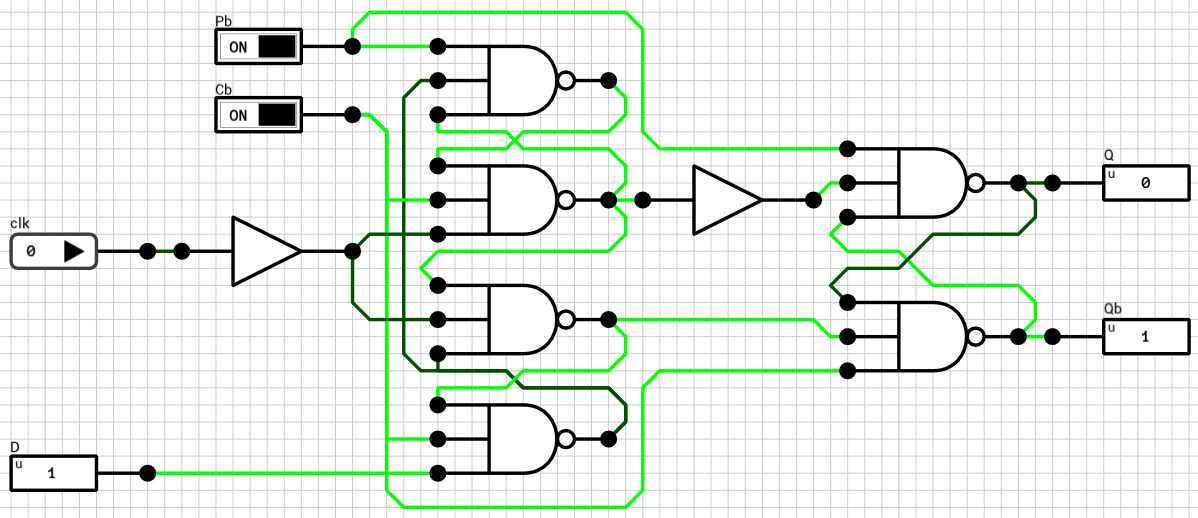
By trial and error, I found that the required delay for the clock signal is 2T (a single AND3 gate or two AND2 gates in series). The final, corrected, DFF circuit is shown in figure 2.
Figure 2: The corrected Positive Edge Triggered D Flip Flop circuit
The testbench works correctly with this circuit. This means that if the controlling circuit sends both signals at the exact same timestep, the flip flop will work correctly. If the clock signal arrives at a later timestep than the D signal it will also, by definition, work correctly.
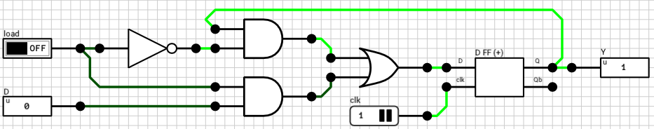
1-bit Register
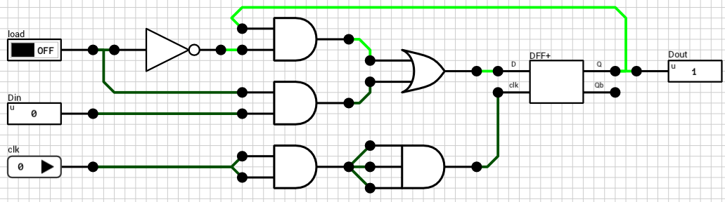
In the same vein, let’s test the original 1-bit register (figure 3). In this case, there’s an extra 1-bit input (load) which determines if the new D value will be written to the flip flop or not. The testbench used to check this circuit is shown in Script 2.
The delay of the critical path of the DFF controlling circuit (i.e. the multiplexer in front of the DFF) is 3T (from load to OR output). So in order to make D and clk arrive at the same time to the DFF component, the clock should be delayed by 3T (one AND2 gate and one AND3 gate in series). Figure 4 shows the new 1-bit register circuit which passes all the tests in the testbench.
Figure 4: The corrected 1-bit Register circuit
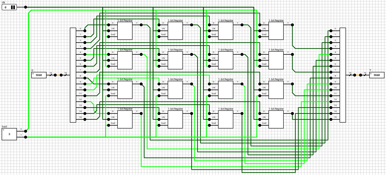
16-bit Register
Once more, the clock in the 16-bit register circuit should be delayed until the D signal is ready to be fed to the 1-bit registers. Only a 16-bit wire splitter exists between Din and the 16 1-bit registers and the wire splitter has a delay of 1T (independent of the number of bits). So by delaying the clock signal by 1T, both Din and clk arrive at the 1-bit registers at the same time. Note that the load signal is already split and directly connected to the registers, so it should be valid when clk and Din arrive.
Script 3 below shows the testbench for the final 16-bit register circuit from figure 5. This time, since the number of possible transistions of the Din signal are way too many to exhaust, I used random inputs for the Din port.
set("clk", 0);
set("Din", 0);
set("load", 3);
simulate();

local D = randBits(16);
set("Din", D);
tick("clk");
assert(get("Dout") == D, "Failed");
tick("clk");

for i=1, 1000 do
  local v = randBits(16);
  local load = randBits(2);

  set("Din", v);
  set("load", load);

  tick("clk");

  local expectedValue = v;
  if(load == 0) then
    expectedValue = D;
  elseif(load == 1) then
    local low = bit.band(v, 0x00FF);
    local high = bit.band(D, 0xFF00);
    expectedValue = bit.bor(low, high);
  elseif(load == 2) then
    local low = bit.band(D, 0x00FF);
    local high = bit.band(v, 0xFF00);
    expectedValue = bit.bor(low, high);
  else
    expectedValue = v;
  end

  assert(get("Dout") == expectedValue, "Failed");

  D = expectedValue;

  tick("clk");
end
Script 3: 16-bit Register testbench
Figure 5: The corrected 16-bit Register circuit
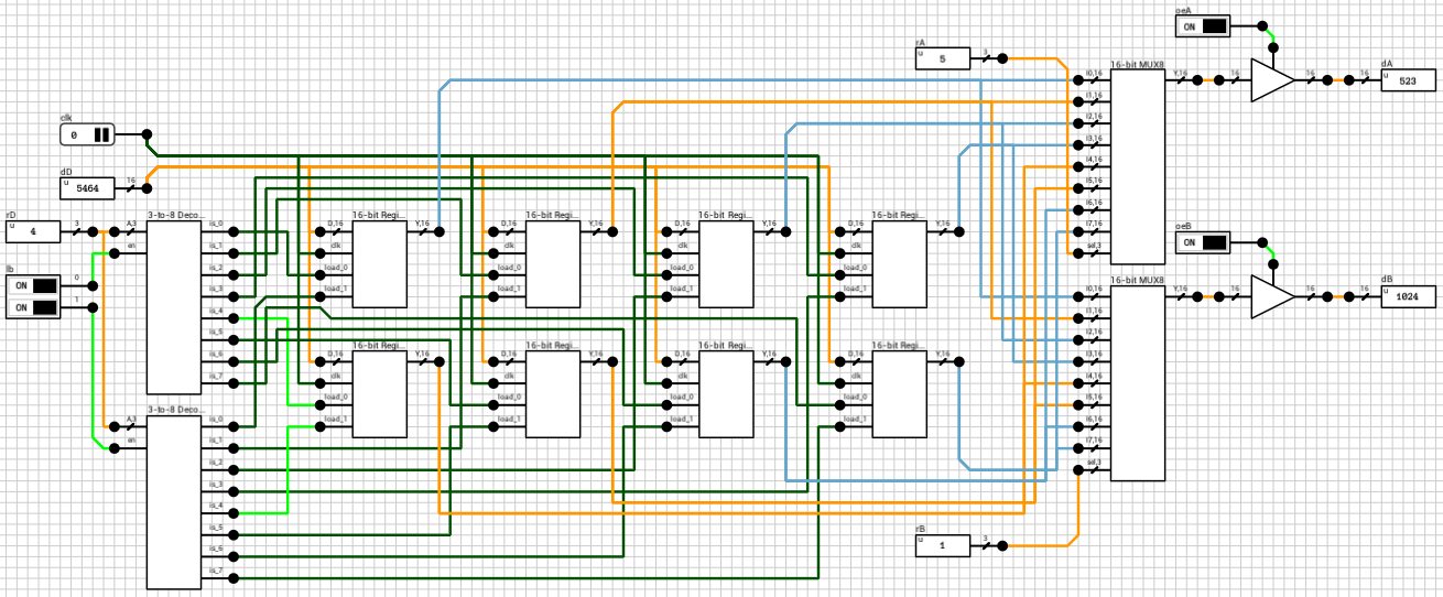
8x16-bit Register file
Finally it’s time to look the actual register file circuit (figure 6). We are only interested in the write part of the circuit, since reading is performed asynchronously (whenever rA, rB, oeA or oeB change, the outputs are immediately updated, without waiting for a clk rising edge).
Figure 6: The original 8x16-bit Register File circuit (write part)
Both dD and clk are directly connected to the corresponding inputs of all 8 registers so it’s probably expected that the circuit will work correctly once we replace the old registers with the new components presented above. Script 4 shows a small testbench.
-- Reset the circuit. Don't touch dD for extra randomness :)
set("rA", 0);
set("rB", 1);
set("rD", 0);
set("lb", 3); -- Write both bytes to simplify testing
set("clk", 0);
simulate();

-- Test 1: Write a random value to register 0.
local v = randBits(16);
set("dD", v);
tick("clk");
assert(get("dA") == v, "Failed");
tick("clk");

-- Test 2: Write a random value to register 1.
local v2 = randBits(16);
set("dD", v2);
set("rD", 1);
tick("clk");
assert(get("dA") == v, "Failed");
assert(get("dB") == v2, "Failed");
tick("clk");
Script 4: 8x16-bit Register File testbench
As always, the circuit is first reset to a known state. rA and rB are pointed to registers 0 and 1 respectively, rD (the destination register) is set to 0 and lb is set to 3, meaning both bytes will be written, to simplify testing.
Test 1 tries to write a new random value to register 0. What’s expected is that when clk rises, the new value should be written to the register and dA should be updated to reflect it. This works correctly, since the registers have been corrected to handle both signals arriving at the same time.
The 2nd test tries to write another random value to register 1, by switching rD to 1 and dD to the new value, at the same timestep. It’s expected that when clk rises, the new value should be written to the register and dB should be updated to reflect it. Unfortunately, this part doesn’t work correctly!
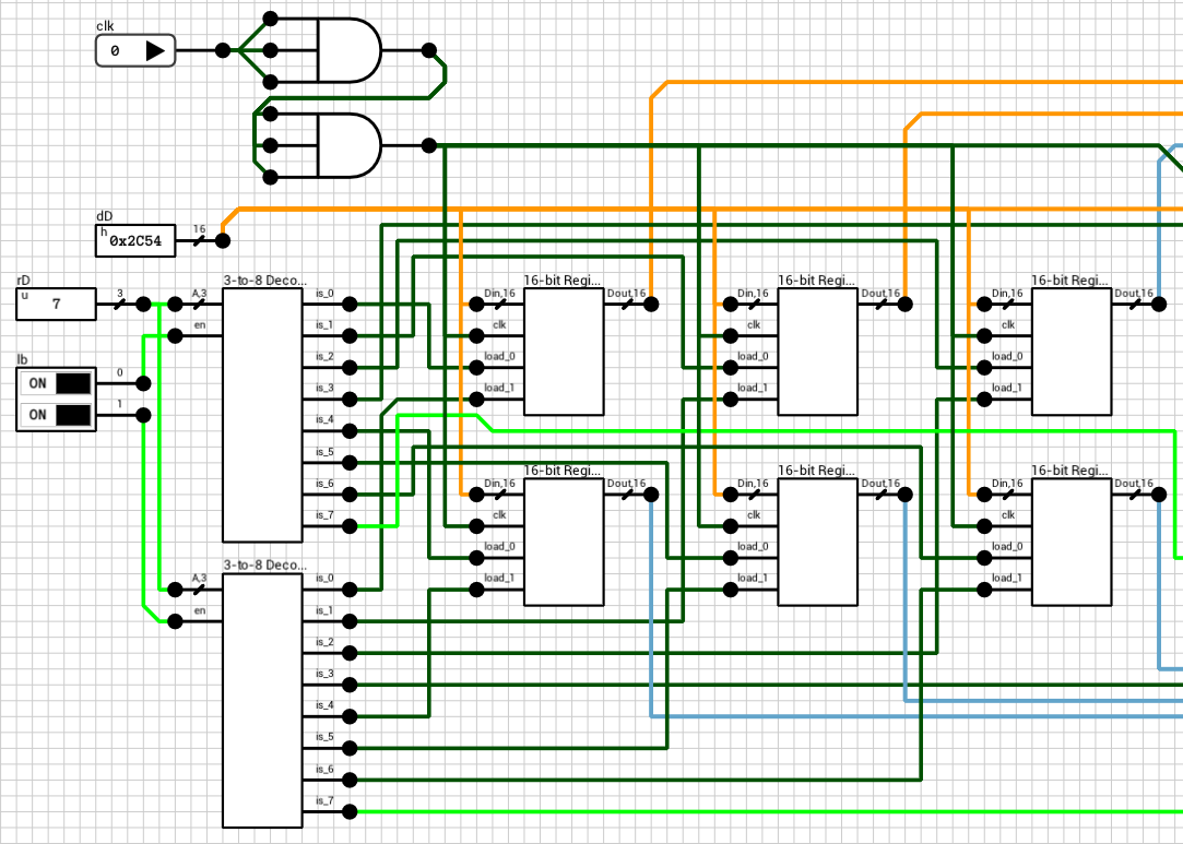
The reason is that there’s a delay on the load inputs of each register. By the time clk and dD arrive at the registers, the old rD is used to select the destination, because the 3-to-8 decoder haven’t had a chance to calculate its new output yet.
Looking at the 3-to-8 decoder (figure 7), the critical path delay is 4T, from A to is (1T for the wire splitter, 1T for the NOT gates and 2T for the AND4 gates). So, delaying the clk signal by 4T should do the trick.
Figure 7: Gated 3-to-8 decoder circuit
Figure 8 shows the final register file circuit. The 4T delay has been added to the clk signal using two AND3 gates.
Figure 8: The corrected 8x16-bit Register File circuit (write part)
Conclusion
If there’s something to keep in mind from this post is that whenever there’s a register/flip flop in a circuit, you should make sure that clock’s rising or falling edge arrives to it at the same time or after the data signal. Otherwise, you might need an extra clock cycle to actually store the new value in the register.
Note that the old version worked correctly in all other aspects. It just needed an extra rising edge to actually write the new value to the registers, which sometimes might be annoying when trying to debug it. Having the register file behave in the way we did in this post will make things a bit easier to debug when this component is used in a larger circuit.
Until the next post, comments/suggestions/corrections are
welcome.
As of yesterday (19 Sept 2016) DLS has its first set of playable levels! 37 to be exact :)
Level types
Currently there are 3 different level types. Combinational circuits, sequential circuits and stream processing circuits.
Combinational circuits
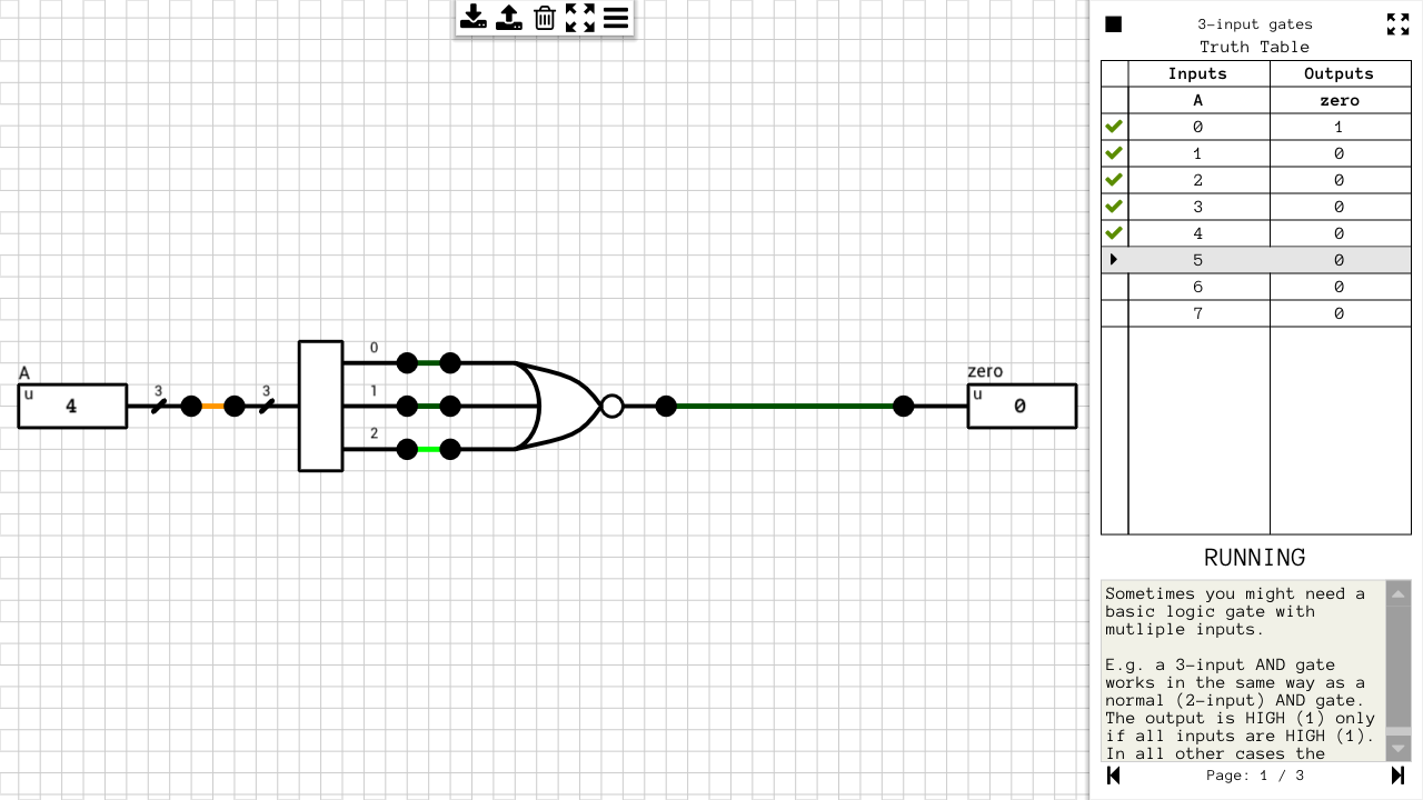
In a combinational circuit level your goal is to build a circuit which, given some specific inputs, will produce the expected outputs combinationally i.e. will react to input changes immediately, without the use of flip flops, registers and clocks. Figure 1 shows such a level.
Figure 1: Combinational circuit level
On the right side of the screen it’s the truth table you are expected to match. The input and output values might be random, depending on the level. E.g. if the inputs are narrow enough to be able to exhaust all possible input values, then the truth table is hardcoded and will never change. Otherwise, the inputs are randomized every time you start the level.
Since there’s no clock involved in these levels, the only property you might want to optimize is the total number of transistors used to create the circuit. More details on this below.
Sequential circuits
In this type of level, your goal is to build a circuit which will produce the expected output at specific simulation timesteps. Figure 2 shows such a level.
Figure 2: Sequential circuit level
The timing graph at the bottom of the screen shows the clock, the input values at specific timesteps and the expected outputs.
Side note: There are two different timelines in DLS: the steady state timeline and the transient (or internal) timeline. Given an initial steady state of a circuit, every change to an input value generates an event at time 0 of the internal timeline. Depending on the type of gates this input is connected to, new events are generated at future internal timesteps, based on the gate’s propagation delay. This cycle of event generation and propagation is repeated until no more new events are generated. At this point the circuit has reached a new steady state and the steady state timeline is advanced. The timing graph in all sequential levels corresponds to the steady state timeline. It doesn’t matter how long it took the result to be calculated, in terms of internal timesteps/gate delays, as long as the circuit reaches a new steady state.
In contrast to the combinational levels, these levels include a clock, but since its value over time is hardcoded, the only property you might want to optimize is the total number of transistors used to create the circuit.
Stream processing circuits
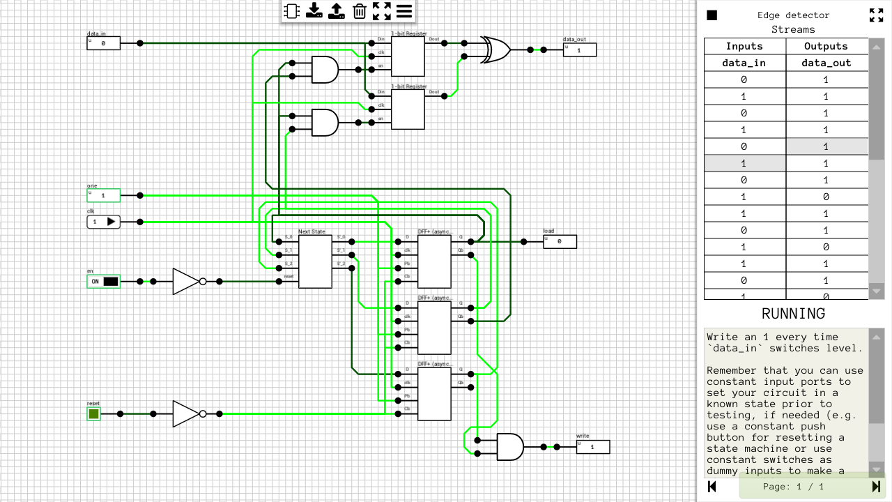
The last type of level is, in my opinion, the most interesting. You get as input a stream of data and a clock. Your goal is to create a circuit which will read the input stream(s) and generate the expected output stream(s). In this case, each input stream has its own load signal and each output stream has its own write signal. Every time a rising edge is detected on one of those, a new value is loaded or written from/to the corresponding port. Figure 3 shows one such level.
Figure 3: Stream processing circuit level
You can implement those circuits in any way you want. This time, the clock is continuously ticking, but since you load and write data at your own pace, one extra property you might want to optimize for is the total number of clock ticks it takes for your circuit to process all the data. E.g. if you are able to produce 2 or more values in the same clock tick, you only have to produce 2 rising edges on the corresponding write output. The same is true for loading the input streams.
Transistor Count and Maximum Clock Frequency
I wanted to add some form of scoring mechanism to all the levels and the total number of transistors used in the circuits is the most common one I could use. The number of transistors for each build-in gate is supposed to be based on a CMOS implementation. E.g. a 2-input NAND/NOR gate requires 4 transistors, an inverter gate requires 2 transistors and a 2-input AND/OR gate requires 6 transistors (4 for the NAND/NOR + 2 for the inverter).
Another way of measuring the efficiency of a circuit is to calculate the delay of its critical path. Knowing the critical path delay, we can estimate the maximum clock frequency a circuit can operate with.
Unfortunately, calculating the critical path of an arbitrary circuit isn’t that simple. As far as I know, all the algorithms used for such a task by logic simulators use a dedicated flip flop component in order to be able to break a sequential circuit into combinational parts and sync points. Knowing that kind of info, one can calculate the critical path of each combinational part. The slowest part is the own which indicates the maximum operating clock frequency.
Since DLS doesn’t have such a dedicated flip flop component, this is nearly impossible to implement. The only way I can estimate the critical path delay of an arbitrary circuit in DLS is by repeatedly simulating the circuit with random inputs and calculating the total internal timesteps it took to produce the outputs. The problem is that in order to reliably estimate the critical path delay this way requires too many simulations, which in turn require extra time.
The advantage of this kind of measurement is that techniques such as pipelining will show their benefit by allowing faster clocks to be used. I’ll reconsider it for a future version.
That’s all for now. Hope to find some more time to work on new levels and different level types. Until then, you can send your feedback
on Twitter.
Since DLS doesn’t support more than 16 bits per wire/pin, I’ll apply the same algorithms on
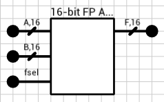
16-bit floating point numbers. I kept the same component names to easily find the connection between the paper and the schematics below. There are also some differences from the paper which I’ll point out when describing the relevant part of the circuit.
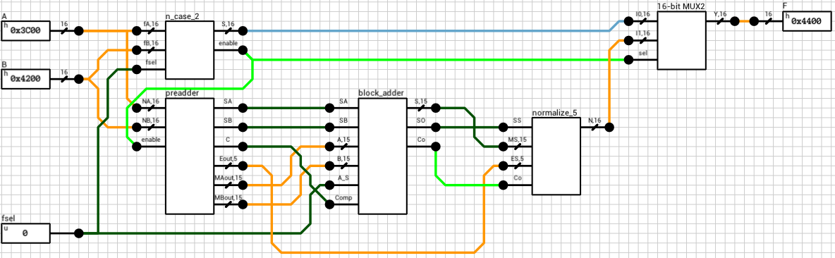
Figure 1 shows the final component. It has 3 inputs (A, B, and fsel) and 1 output (F). A and B are the two 16-bit floating point numbers. fsel is the function select signal, with 0 for addition and 1 for subtraction. F is the result of the operation.
Figure 1: 16-bit Floating Point Adder component
Step 1: Check for a special case
The first step is to check if we have a special case. Special cases are considered all the cases for which the result of the operation between the 2 inputs can be determined without performing the operation. I.e. adding 0 to a number results in the number itself, adding opposite sign infinities results in a NaN, etc. (see the paper for all the cases).
The block handling this part is called n_case (figure 2). It has 2 outputs, S and enable. S is the result of the operation if a special case is detected, otherwise Undefined. enable is used to turn on the rest of the circuit in case the current combination cannot be handled by this block.
Figure 2: n_case block
There are 2 bugs in the n_case code from the paper.
First, the classification of inputs A and B (intermediate signals outA and outB) are wrong when A or B are powers of 2 (0 < E < 255 and M = 0). Both codes on pages 22 and 96 end up producing a value of 000 for outA and outB, meaning the numbers are zero. In order to fix this problem, we just have to ignore the mantissa, in case E is in the range (0, 255) (or (0, 31) in our case of 16-bit numbers).
The second bug has to do with the treatment of B. The n_case block takes as input only the two numbers and ignores the selected operation. If fsel is 1 (subtraction), B’s sign should be reversed before checking the special cases. If we don’t do that, subtracting any number from 0 will result in the number itself, instead of its negative value (e.g. 0 - 1 = 1).
Both problems have been addressed in the circuit shown in figure 2. Other than that, the rest of the circuit consists of simple checks for each case. I decided to reverse B’s sign before making any checks, in case of subtraction. This means that 0 - 0 results in a negative zero, because the case where A is zero has higher priority than the case where B is zero. Not much of a problem, but it should be mentioned.
Step 2: Prepare for addition
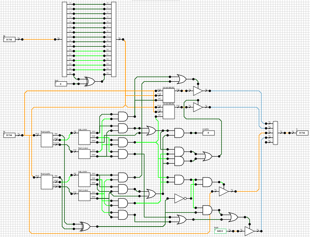
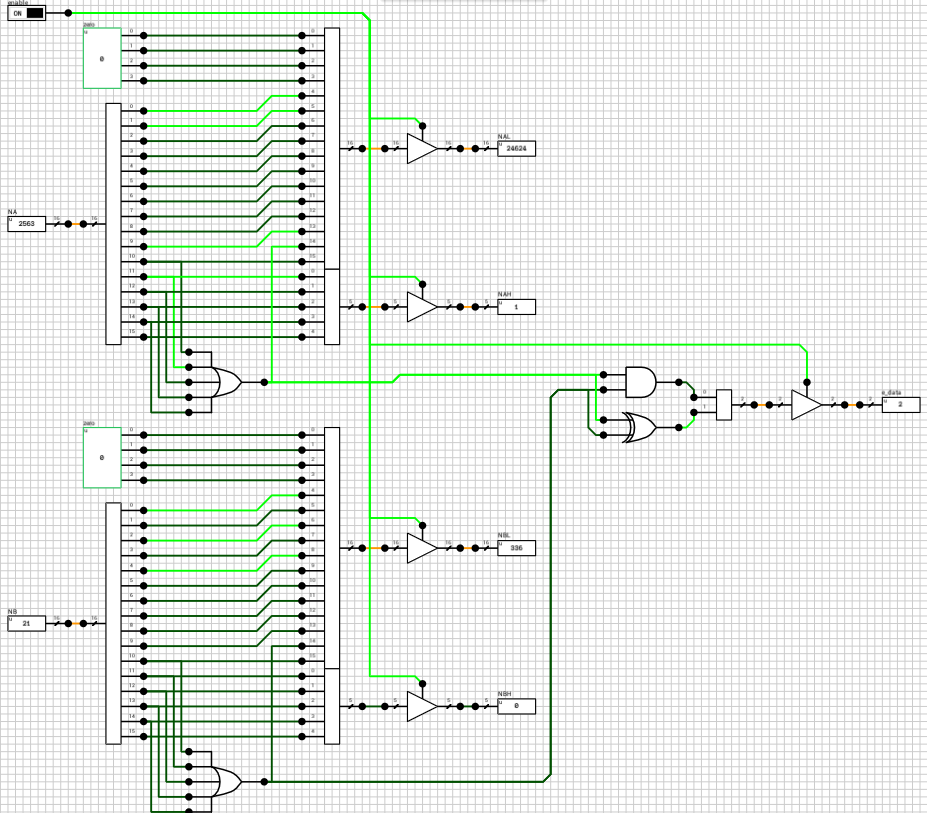
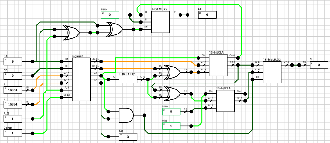
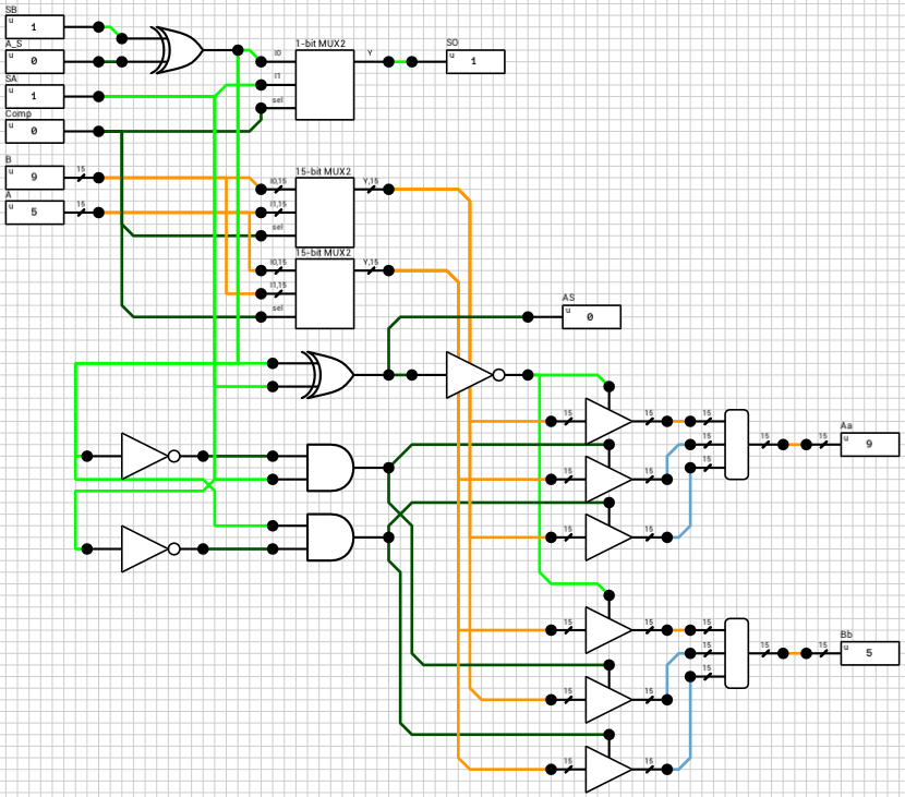
If the enable output of the n_case component is HIGH, it means that both A and B are regular numbers (normals or subnormals). Before being able to add them together, we have to align their decimal points. This is done by finding the exponent of the largest number and shifting the mantissa of the other to the right, until both exponents are equal. Remember that shifting the decimal point to the left means that the mantissa is shifted to the right. Also, for each shifted position, the exponent is incremented by 1. This part is handled by the preadder component (figure 3).
Figure 3: preadder block
The preadder takes as input the two 16-bit numbers and the enable signal from the n_case component. First it expands both numbers to 21 bits, by introducing the implicit bit (1 for normals and 0 for subnormals) and adding 4 guard bits at the end. This is done in the selector (figure 4). The selector also outputs a 2-bit signal e_data indicating the type of both numbers (00 when both are subnormals, 01 when both are normals and 10 in case of a combination).
Figure 4: preadder selector
Note that the expanded 21-bit numbers are broken into 2 signals. A 16-bit for the lower part and a 5-bit signal for the higher part.
After expanding the numbers, depending on the value of e_data the correct path is chosen. If both numbers are subnormals, they are handled by the n_subn block (figure 5). In this case the output exponent is 0 (which the same for both numbers). The two mantissas are compared and the largest one is placed on MA and the other on MB. If the A input is larger than B, then Comp is HIGH, otherwise it’s LOW.
Figure 5: preadder n_subn
Side note: I’ve used a 16-bit magnitude comparator to compare the 2 mantissas, eventhough the extended mantissas are 15 bits wide. The 16th bit is taken from the exponent, because I know that both numbers are subnormals and thus have an exponent of zero.
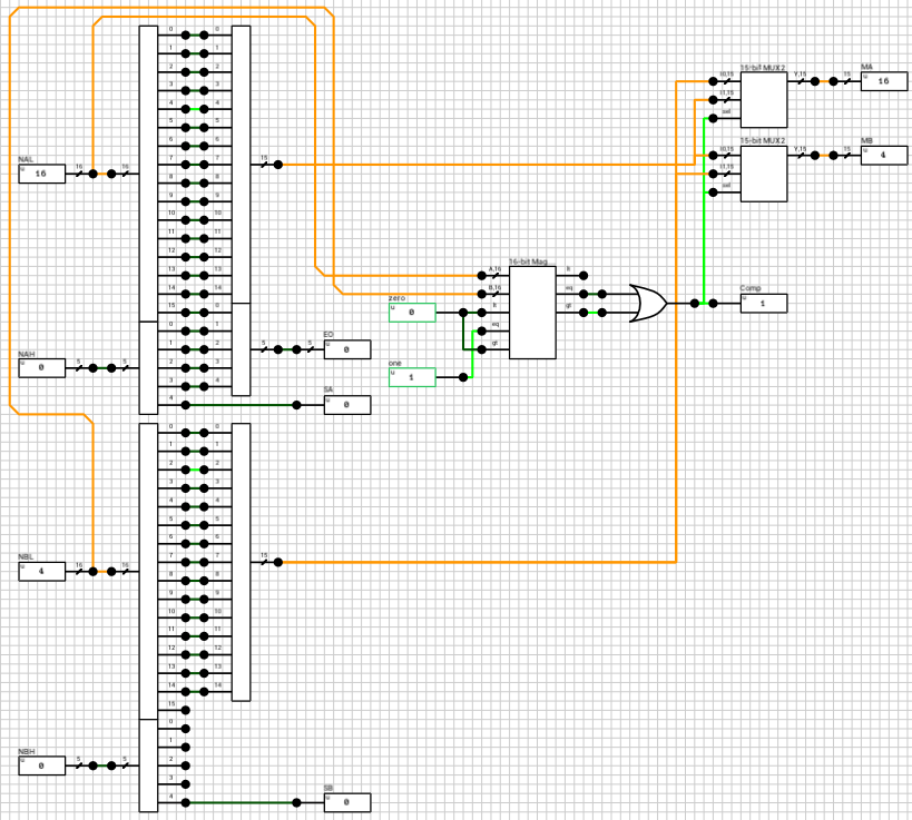
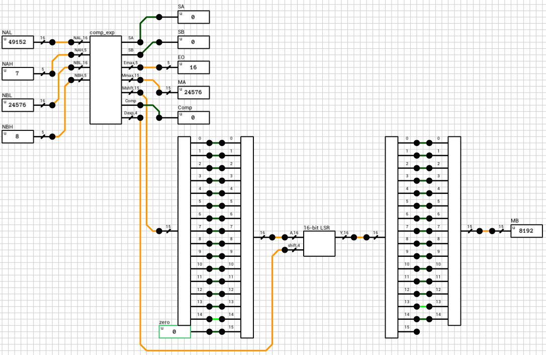
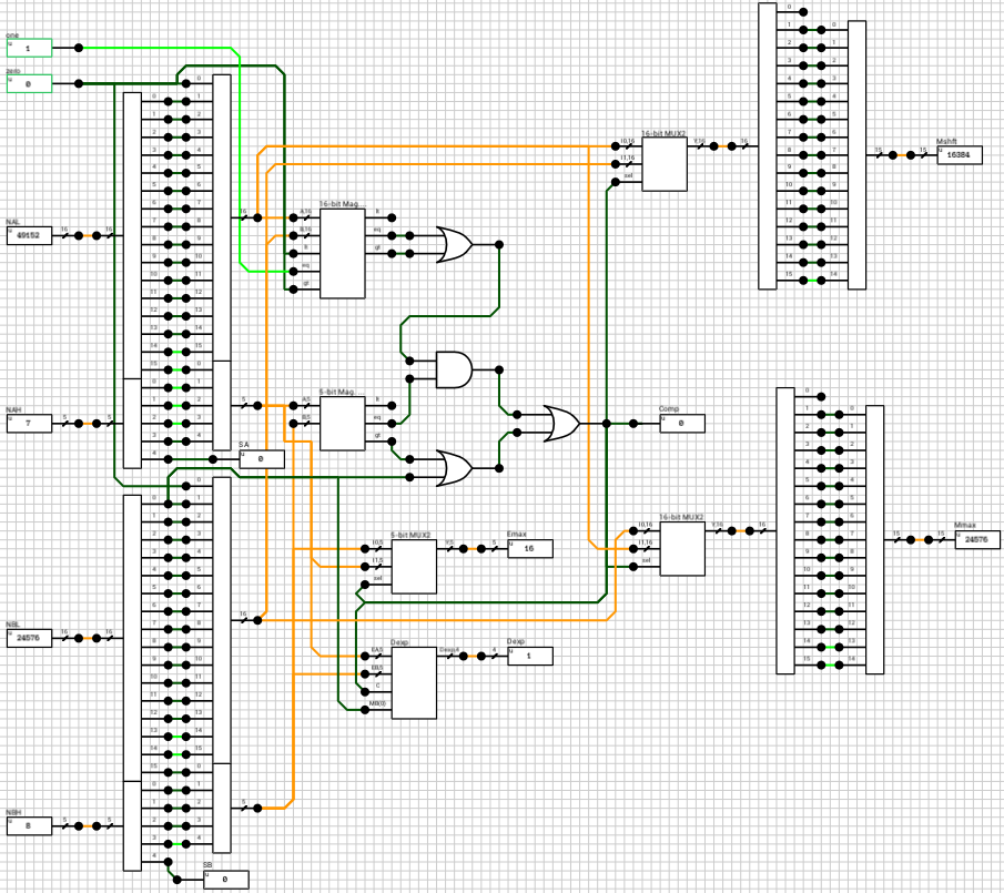
If the numbers are both normals or a combination of a normal and a subnormal, they are routed to the n_normal block (figure 6 and figure 7). Again both numbers are compared and the output exponent EO is set to the largest exponent. MA holds the largest number’s mantissa. The smaller mantissa (Mshft output from the comp_exp component) is shifted to the right based on the difference of the two exponents.
Side note: The comp_exp component uses the same 16-bit magnitude comparator as in the previous case. This time, since the exponents are non-zero, I made the 1st bit equal to 0 and the rest of the bits come from the extended mantissa.
After this step, all outputs from n_subn and n_normal are routed to the mux_adder and the final outputs of the preadder are calculated, based on e_data.
The outputs of the preadder block are the following:
SA and SB: The signs of the two numbers
C: 1-bit flag indicating if number A is larger than number B
Eout: The final exponent, equal to the largest exponent
MAout: The mantissa of the largest number
MBout: The mantissa of the smallest number
Step 3: The addition/subtraction
We now have both numbers in the order and the format required to perform the selected operation. Since both exponents are equal, the only thing required is to add/subtract the mantissas. This is handled by the block_adder component (figure 8). The block_adder takes as input the two signs, SA and SB, the two mantissas A and B, the selected operation (0 for addition, 1 for subtraction) and the Comp flag which indicates if A is larger than B.
Figure 8: block_adder
The signout block (figure 9) is responsible for calculating the sign of the result, the true operation to be performed between the two inputs and for reordering the inputs in case the true operation is different than the selected operation. The true operation is the actual operation to be performed between the two inputs. I.e. if we subtract a negative number from a positive number, the true operator is addition, which is different than the selected subtraction.
Figure 9: block_adder signout
The final addition/subtraction is performed using a trimmed 16-bit CLA. The circuit is similar to the one presented in the previous article, with the only difference being that the 16-th bit of the result is used as the carry out of the addition and the sum is only 15 bits wide.
Step 4: Normalization
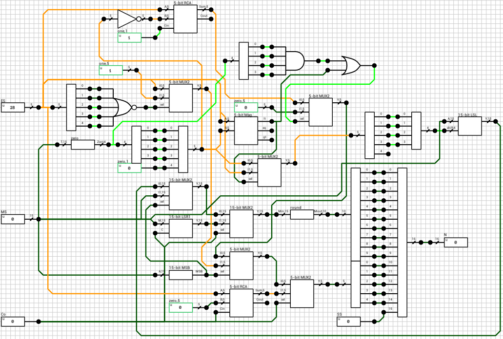
We now have all the parts necessary to reconstruct the result. Figure 10 shows the normalization block (norm_vector from the paper).
Figure 10: norm_vector
It might seem a bit more complicated than necessary so I’ll try to describe the circuit in pseudocode below. The job of this component is to normalize the mantissa and correct the exponent accordingly. It gets as inputs the sign of the result (SS), the exponent (ES), the mantissa (MS) and the carry out of the addition (Co). Note that this part is very different than the one found in the paper. I probably didn’t understand the VHDL correctly and my attempts to map it directly to circuit ended up producing invalid results. The circuit shown in figure 10 seems to behave correctly in all tested cases.
There are several cases to consider when normalizing the mantissa. The code below shows all of them in pseudocode (assume a combined 16-bit number ZX.YYYYYYYYYYYYYY, where Z = Co and X = MSB(M))
if Z == 1 then
    E' = E + 1
    M' = M >> 1 // M' = 1.XYYYYYYYYYYYYY
else
    if X == 1 then
        if E == 0 then // subnormal + subnormal = normal
            E' = 1
            M' = M // M' = 1.YYYYYYYYYYYYYY
        else
            E' = E
            M' = M // M' = 1.YYYYYYYYYYYYYY
        end
    else
        lz = leading_zeroes(M)
        if E < lz or lz == 15 then
            E' = 0
            M' = M << E // Shift the mantissa to the left until the exponent becomes zero
        else
            E' = E - lz
            M' = M << lz // Shift the mantissa to the left until an 1 appears on the MSB
        endif
    endif
endif
Hope it’s a bit more clear than the circuit :)
There are 2 special cases to consider. When adding two subnormal numbers, the result might end up being a normal (e.g. 0x0200 + 0x0200 = 0x0400 which is the smallest normal). In this case Z = Co = 0, X = MSB(M) = 1 and E = 0. The mantissa is already normalized (has an one at the MSB), so the exponent needs to be incremented to 1. If it’s left at 0, the result will be wrong when rounding the mantissa (see below).
The other case is then both X and Z are zero. In this case we have to shift the mantissa to the left until it becomes normalized or until the the exponent gets to 0. This can happen if the number of leading zeroes in the mantissa is larger than the exponent or if the mantissa is 0 (lz = 15). If the mantissa is zero at this point, it means that the result is 0 independently of the exponent (i.e 0x4000 - 0x4000 = 0 eventhough ES = 0x10).
Side note: The leading_zeroes component has been implemented using a 32k x 4-bit ROM.
Other than those 2 cases, the rest should be easily derived from any explanation on floating point addition.
The final step after calculating E' and M' is to round the mantissa. This involves ignoring the implicit bit (15-th bit) and rounding the guard bits. In order to keep things as simple as possible I decided to just cut off the guard bits, which is effectively rounding towards zero.
The final floating point adder circuit is shown in figure 11.
Figure 11: 16-bit Floating Point Adder
Thanks for reading. Comments and corrections
are welcome.
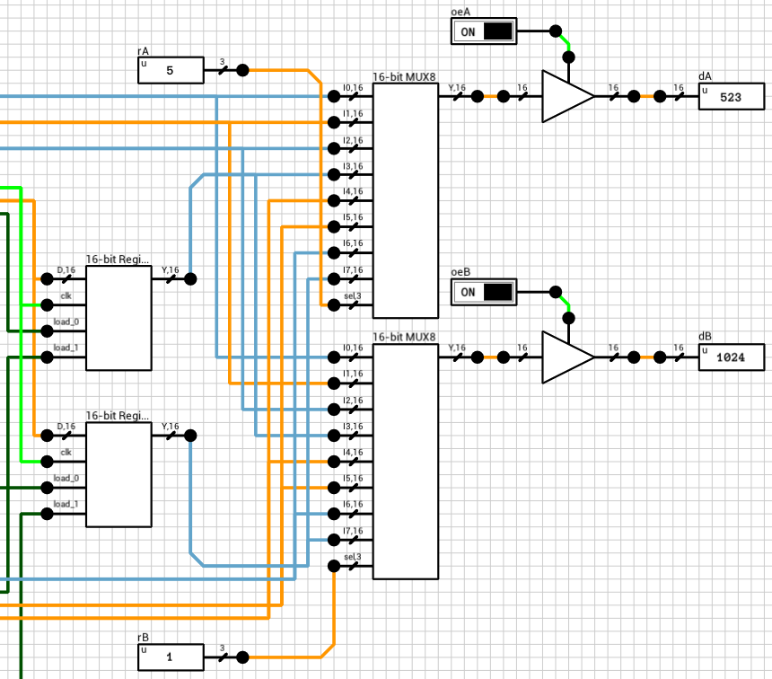
The goal of today’s post is to build a 8x16-bit register file, i.e. a bunch of memory elements packaged as a single component. Figure 1 shows the final component we are going to build. It can read two registers asynchronously and write one of them on the rising edge of the supplied clock.
Figure 1: 8x16-bit Register File component
The first input is the clock (clk). The 16-bit value dD will be written to the register pointed by rD on the rising edge of the clk input. Since the registers will be 2 bytes wide, each byte can be independently written via the lb_0 and lb_1 inputs (lb = load byte).
Inputs rA and rB are the two registers we are interested in reading. Their current value will be available on the dA and dB outputs. Note that these 2 won’t be synchronized to the clk input. They can change at any moment and their respective output will be updated (almost) immediately.
Finally, oeA and oeB inputs (oe = output enable) control whether the corresponding output will hold the current value of the selected register, or if it will float. This way, we can use multiple instances of this register file to increase the number of available registers in a circuit, by combining all their outputs on a common bus. More on this at the end of the post.
Positive edge triggered D flip flop
Let’s start small. The basic building block for this component is the “Positive Edge Triggered D Flip Flop” shown in figure 2. It consists of three cross-coupled active LOW SR latches. Every time the clk input goes from LOW to HIGH, Q is updated to mirror the input D.
Figure 2: Positive Edge Triggered D Flip Flop circuit
Qb is the complement of Q. It won’t be used later, but it’s there for completeness. The same flip flop can be used to build other kinds of circuits where Qb might be needed. The latches are connected in a way that the Q output is updated only on the transition of the clk input from LOW to HIGH (positive edge). In all other cases, no change on the D input will affect the Q output. For additional details take a look at the wikipedia article on
flip flops (paragraph “Classical positive-edge-triggered D flip-flop”).
1-bit Register
The flip flop from figure 2 can hold 1 bit of data. The clk input doesn’t need to be an actual clock. Any kind of 1-bit input can be used as a clock and it will be updated on its rising edge. In cases where the clk input is actually a free-running clock, we might have a problem if we don’t want to update its contents on the next rising edge. E.g. the wire connected to the D input changes value but we don’t want to store it in the flip flop on the next clock tick.
Figure 3 shows how this can be accomplished. By using a 2-input mutliplexer in front of the D input, with the first MUX choice being the old value and the second choice being the new value, we can select whether we want to update the flip flop or not, via the new load input.
Figure 3: 1-bit Register circuit
In order to distinguish this circuit from the flip flop shown above, I’ll call it an 1-bit Register.
Side note: I’ve created the mutliplexer using 2 AND and 1 OR gates instead of 2 tristate buffers and a 2x1-bit bus, as shown in the ALU post. This is because the tristate MUX has a small glitch which affects the rest of the circuit (at least in DLS). When changing the sel input of the tristate MUX, there’s a simulation timestep where both bus inputs are active at the same time. In such cases the buses in DLS are configured to output an Error value. If the output of the bus is connected to the D input of the flip flop, we might end up in an invalid state, from which it’s impossible to get out of. In the ALU circuit this wasn’t a problem since all components were combinational and they correctly handled Error inputs.
16-bit Register
Expanding to 16 bits is easy. We just use 16 instances of the 1-bit Register component, wire everything together and we are done. Figure 4 shows the 16-bit Register circuit.
Figure 4: 16-bit Register circuit
As I mentioned at the beginning of the post, since the register is 16 bits wide (2 bytes), we might want to control (write) each individual byte separately. This is the reason the load input is 2 bits wide. Each bit controls one of the bytes. If it’s not obvious from the figure, load_0 is connected to the load inputs of the first 8 1-bit registers and load_1 is connected to the load input of the other 8 1-bit registers.
Side note: The first time a register is initialized, both bytes should be written. The initial state of the D flip flop produces an Undefined output (because the clk hasn’t ticked yet). Since we don’t mask/split the register output to separate the individual bytes, having only 8 of the 16 bits initialized and the rest in an Undefined state will produce an Undefined value on the Y output. This is because, if at least 1 of the inputs on a wire merger is equal to Undefined or Error, the rest of the bits are ignored and the special state is propagated to the output.
The Register File
With the 16-bit Register component ready, we can now build a small register file. To keep things as simple as possible, we’ll use only 8 registers and (as mentioned in the intro) we’ll add a way to mask the outputs in order to be able to cascade multiple instances of this circuit to build larger files. Figure 5 shows the complete circuit. It might be a bit difficult to read, so I’ll break it up into parts, with zoomed in screenshots.
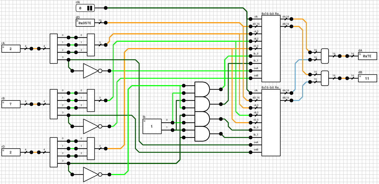
Figure 5: 8x16-bit Register File circuit
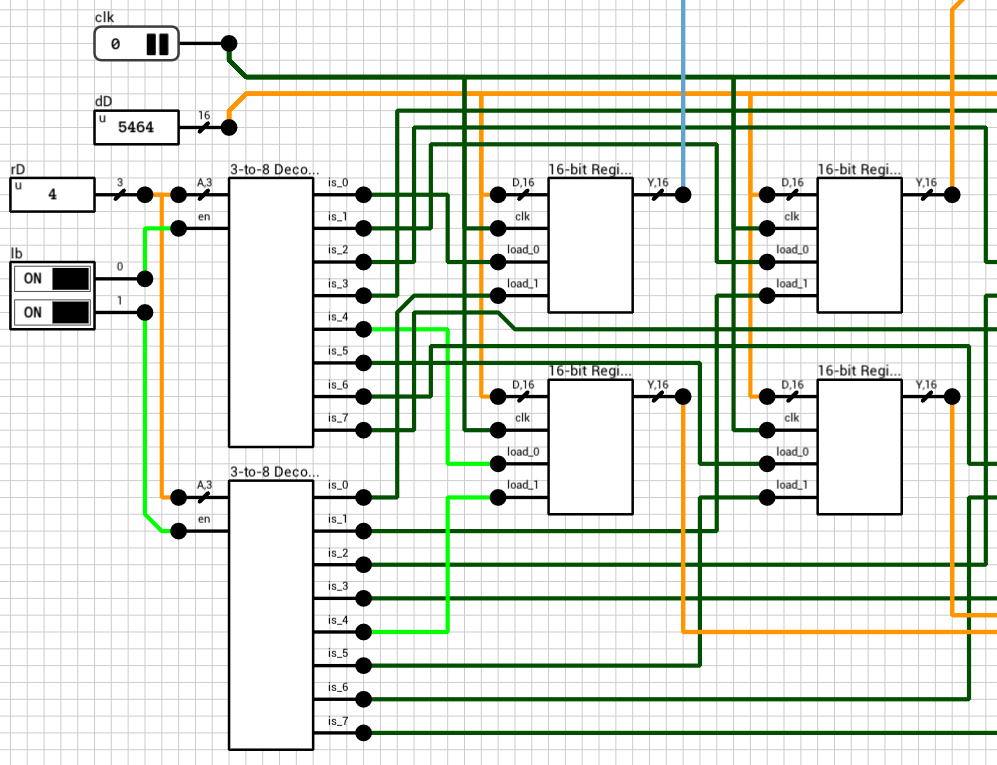
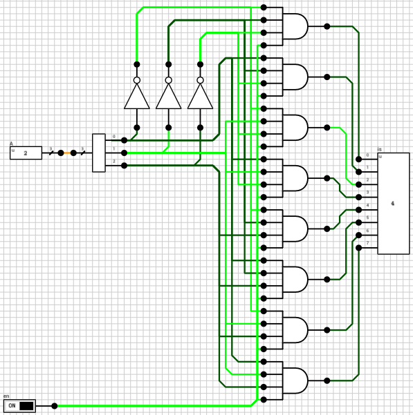
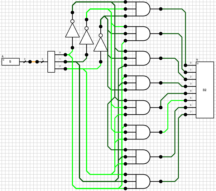
Figure 6 shows the write part of the circuit. clk is the clock and it’s routed to all the clk inputs of the 8 registers. dD is the 16-bit value we want to write to the rD register and it is again connected to the D inputs of all the registers. The 3-bit rD input is decoded using gated 3-to-8 decoders, one for each byte, based on the lb input. A gated decoder (figure 7) works the same way as the decoder we saw in the ALU post, with the only difference being that when its en input is LOW, all outputs are LOW.
Figure 6: The *write* part of the circuitFigure 7: 3-to-8 Gated Decoder
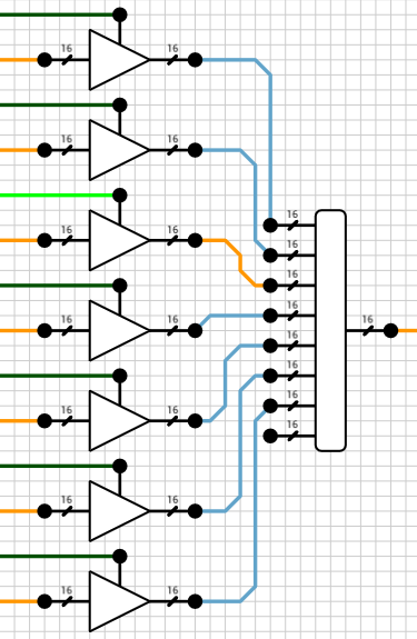
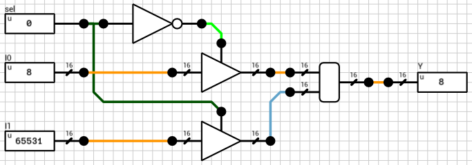
Figure 8 shows the read part of the circuit. All register outputs are routed to two 16-bit 8-input mutliplexers (figure 9). rA and rB are used as the sel input to the two MUXes. MUX outputs are connected to 16-bit tristate buffers, with the control pins connected to the oeA and oeB inputs.
Figure 8: The *read* part of the circuitFigure 9: 16-bit 8-input MUX
Note that in this case, since the MUX is after the flip flops, we can use tristate buffers. As long as the output of the register file isn’t connected to another register, there shouldn’t be a problem. If there is, we can always come back and replace the MUX with an AND/OR version.
Larger register files
The component presented above (figure 5) can be used to build both wider and deeper register files. Unfortunately, DLS doesn’t currently support bit widths larger than 16 bits per wire/pin, so building (e.g.) a 32-bit register file will end up in a mess of wires :) It’s possible, but you’ll need double the IO pins and wires.
Instead of building a wider file we’ll build a larger/deeper one, with 16 registers, using two instances of the component. In this case rA, rB and rD should be expanded to 4 bits, with their MSB used to select the correct file, by turning on or off the corresponding load and oe inputs. The dA and dB outputs of the two instances are connected on one bus each and then routed to the final outputs. Figure 10 shows the final 16x16-bit register file circuit.
Figure 10: 16x16-bit Register File circuit
Note that in this circuit there’s no output enable inputs since I assumed this component won’t be used to build even larger components. If this is the case, both oe inputs should be exposed to correctly handle cascading.
That’s all for now. Thanks for reading. As always, comments and corrections
are welcome.
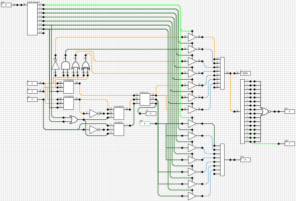
Having implemented an adder, the next step is… to use it in a larger circuit :) Today I’ll try to describe the process of creating a simple Arithmetic/Logic Unit (ALU) in DLS, using the 16-bit CLA from the last post.
ALUs typically support several different functions, instead of just additions, and also output several extra flags to describe the result of the selected function (I think that’s the reason Logic is in the title). The ALU I’ll present will also support 4 bitwise operations and subtraction. Multiplication, division and arithmetic/logical shifting will (probably) be discussed in a future article, as I don’t think they are necessarily a good fit for an ALU (e.g. multiplication can be performed algorithmically in mutliple cycles using repeated additions and shifting might be needed outside the ALU in order to support shifting its result in the same cycle).
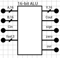
Figure 1 shows the final ALU as a component. It has 4 inputs and produces 5 outputs. Inputs A, B and Cin should be familiar from last time. fsel is used to select the function we want to execute on the other inputs. Table 1 shows the 7 supported functions and their corresponding fsel value. Note that there’s a spare slot (fsel = 7). This can be used later to expand the ALU with one extra function, but we must also take care to produce predictable results in case fsel is set to 7 by the user.
Figure 1: 16-bit ALU component
fsel
Description
0
NOT(A)
1
AND(A, B)
2
OR(A, B)
3
XOR(A, B)
4
A + B + Cin
5
A - B - Cin
6
B - A - Cin
Table 1: ALU’s function table
The component’s outputs are:
Y: the 16-bit result of the selected function
Cout: the output carry of the selected function (if any)
zero: when HIGH it means that Y is zero
sign: the most significant bit of Y
ovr: when HIGH it means that an overflow has occured and Y is invalid. It can happen when (e.g.) the addition of 2 positive numbers produces a negative result.
Output buses and fsel decoder
The way the ALU will be implemented is by calculating all the supported functions in parallel and have a bus at the end which will select the correct output based on the current value of fsel. Figure 2 shows the Y bus. There are 7 different results calculated and each one of them is connected to a 16-bit tristate buffer. All tristate-buffers are then connected to a 8x16-bit bus.
Figure 2: Y output bus
Despite the fact that there are only 7 functions, because fsel is 3 bits wide I used a 8x16-bit bus instead of a 7x16-bit bus, to be able to expand the ALU later. Note that the last bus input isn’t connected to anything and will, by default, have an Undefined value. So, for fsel = 7, Y = Undefined.
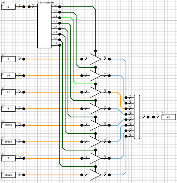
In order to control the 7 tristate buffers, we first need to decode fsel. A 3-to-8 decoder does the job (figure 3). It has only one input (a 3-bit value) and 8 1-bit outputs. When the i-th output is HIGH, it means that the input number is i. Only one of the outputs can and will be HIGH for any given input value.
Figure 3: 3-to-8 decoder
Bitwise operations
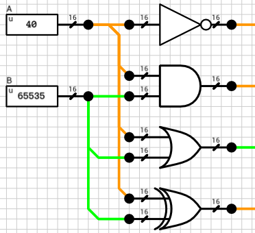
The first 4 functions are easy to implement, especially in the latest version of DLS which supports multi-bit standard gates. Figure 4 shows the subcircuit used to calculate those functions.
Figure 4: Bitwise functions
Only a single multi-bit gate is needed for each case. The outputs are routed to their respective tristate buffers we saw earlier. None of these functions make use of the Cin input, so it’s ignored.
Addition/Subtraction
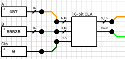
The 5th function is the addition of the two inputs taking into account Cin (Y = A + B + Cin). Using the 16-bit CLA adder we created in the previous article, we can easily calculate both Y and Cout for this case (figure 5).
Figure 5: Addition
Calculating the difference of 2 two’s complement binary numbers A and B can be done using the same 16-bit CLA. If we take into account that A - B = A + (-B) and -B = NOT(B) + 1, where NOT(B) is the one’s complement of B, Y = A - B ends up being translated to Y = A + NOT(B) + 1.
This means that in order to use the CLA for subtraction it is required to invert B and Cin. Cin needs to be inverted because A - B - 1 = A + NOT(B) + 1 - 1 = A + NOT(B). Finally for fsel = 6 we need to swap A and B before doing any of that. Table 2 shows the 3 different cases.
fsel
CLA.A
CLA.B
CLA.Cin
Y
4
A
B
Cin
A + B + Cin
5
A
NOT(B)
NOT(Cin)
A - B - Cin
6
B
NOT(A)
NOT(Cin)
B - A - Cin
Table 2: CLA inputs and expected result for functions 4, 5 and 6
There are 2 ways to implement the subcircuit which will control the CLA inputs. Either use three 4-input multiplexers (MUX), one for each CLA input, with an invalid/duplicate sel code, or break the decision tree into 2 steps and use only 2-input MUXes (which avoids having invalid/duplicate sel codes). I’ll describe the second method.
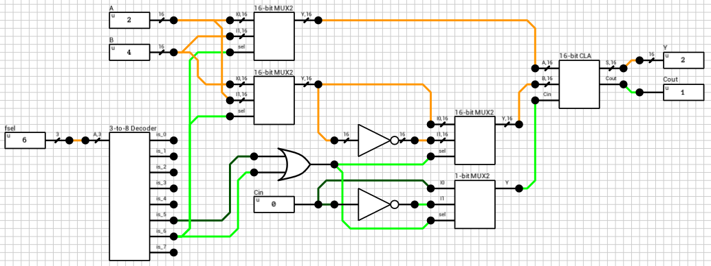
The first step is to decide if we need to swap A and B. This is done by using two 16-bit 2-input multiplexers (figure 6), with their sel input connected to the 7-th output pin of the fsel decoder (because only function 6 needs reversed inputs). The 1st MUX has I0 = A and I1 = B. The 2nd MUX has I0 = B and I1 = A. When fsel = 6, the 7-th output pin of the decoder will be HIGH and both MUXes will select their I1 inputs (B and A respectively). In all other cases, both MUXes will select their I0 inputs (A and B respectively)
Figure 6: 16-bit 2-input MUX
The second step is to check if we need to invert B and Cin. This is done by ORing the 6th and 7th output pins of the fsel decoder (meaning that the operation is a subtraction) and using the result as input to 2 multiplexers; a 16-bit one for the second operand and a 1-bit for Cin. Finally the multiplexer outputs are connected to the CLA. Figure 7 shows the relevant subcircuit.
Figure 7: Final ADD/SUB subcircuit
Cout
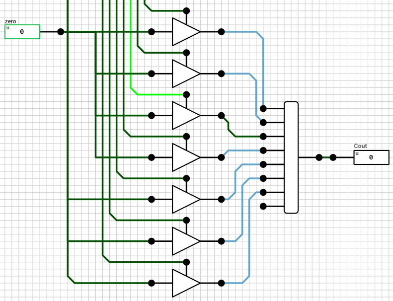
Up to this point I’ve only talked about the Y output, because this was the most complicated of them. The 2nd output is Cout. For fsel = 0,1,2,3, Cout will always be 0, because the operations do not produce a carry. For fsel = 4,5,6, Cout is the carry output of the CLA. Using 1-bit tristate buffers and a 8x1-bit bus, as with Y, will do the trick. Figure 8 shows the relevant subcircuit.
Figure 8: Cout subcircuit
NOTE: Input ports with a green border, such as the zero port in the above figure, are constants. This means that when the circuit is turned into a component, those ports will not appear as inputs pins on the component.
Flags
The last thing we have to implement is the calculation of the 3 flags I mentioned above, zero, sign and ovr.
zero can be calculated by NORing all the bits of the Y output. In DLS this requires using a wire splitter to get the individual bits of the wire and a 16-input 1-bit NOR gate. If any of the bits of Y is HIGH, Y is not zero and NOR will return LOW. If all the bits of Y are LOW NOR will return HIGH.
sign is the MSB of Y. Since we already used a wire splitter to calculate the zero flag, we can grab the 16-th pin and connect it to the sign output port.
ovr is a bit more complicated. Overflow can only happen when, adding two numbers with the same sign produces a result with a different sign (
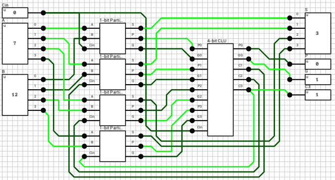
reference). In our case we should also take into account the input carry. The easiest way to see if overflow has occurred is inside the adder. By comparing the carry into the sign bit with the carry out of the adder we can detect overflow. In order to implement this method, we have to revisit the CLA and make a small adjustment. Figure 9 shows the new 4-bit CLA. The carry into the sign bit is the C3 output of the 4-bit CLU.
Figure 9: The new 4-bit CLA with the C3 output.
After replacing the four 4-bit CLAs in the 16-bit CLA circuit with the new components, the ovr flag is calculated by XORing the C3 output of the last 4-bit CLA with the final carry out of the adder (figure 10).
Figure 10: The new 16-bit CLA with the `ovr` output.
Complete circuit
Figure 11 shows the final circuit. I haven’t measured the delay of the various functions, and I suspect there might be a couple of changes which might help in this area, but since the article is getting really long, it’ll do for now. Knowing the worst case delay of the ALU might be needed in cases where correct timing of the results is required.
Figure 11: The final 16-bit ALU circuit.
Thanks for reading. Comments and corrections
are welcome.
PS. If you find it hard to read the schematics due to the large amount of wires, remember that wires meeting at a T junction are connected, and wires crossing each other are not connected. Hope it helps :)
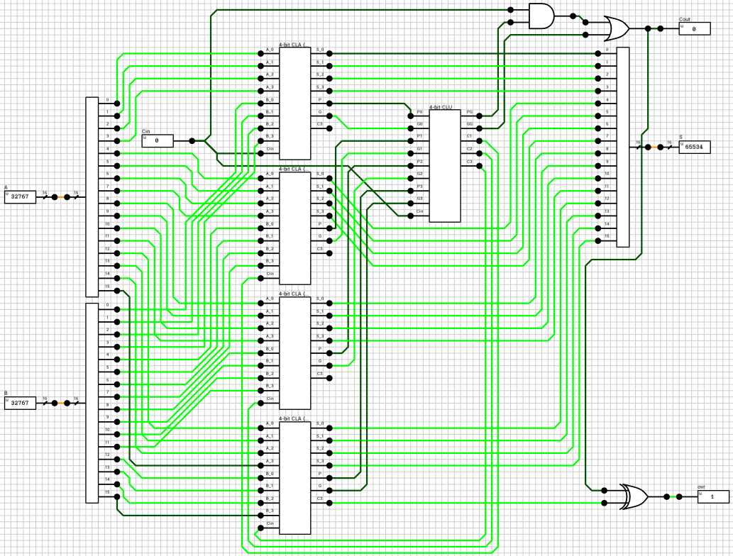
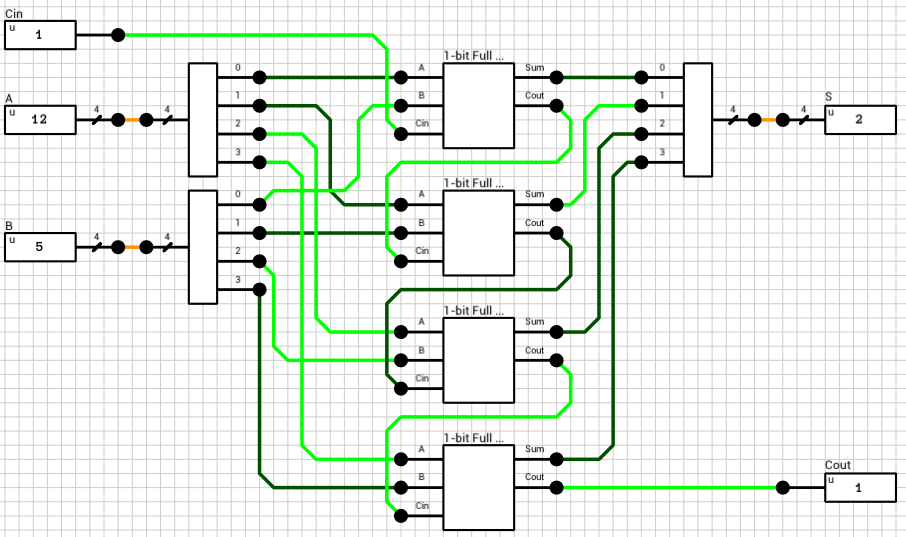
Last time I presented 2 different implementations of a 4-bit adder. The Ripple Carry adder (RCA from now on) was a bit slower in terms of gate delays compared to the Carry Lookahead adder (CLA). Today I’ll try to reuse those circuits as components in order to build 2 different versions of a 16-bit adder.
Before turning the circuits into components, and in order to keep the overhead of splitting and merging fat wires using Wire Splitters and Mergers, I replaced the 4-bit single-pin inputs A and B with 4-bit 4-pin inputs. The difference is that the generated component will have 8 individual 1-bit inputs (excluding Cin) for A and B. The same is done to the S output.
Figure 1 shows the simplified 4-bit RCA circuit and figure 2 shows the simplified 4-bit CLA circuit. Also note that the Cout output of the 4-bit CLA has been removed because it won’t be used in the 16-bit circuit.
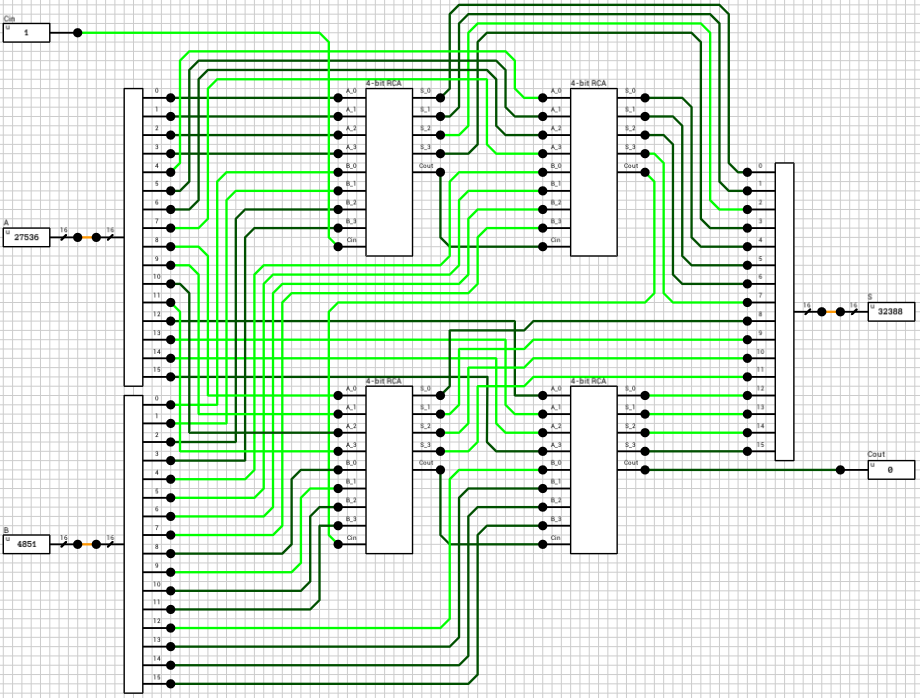
Figure 3 shows the 16-bit RCA circuit. It includes 4 instances of the 4-bit RCA component, connected in series (if it’s not obvious from the image, the order is top left -> top right -> bottom left -> bottom right; just follow the carries). If we take into account that each 4-bit RCA includes 4 1-bit Full Adders, this circuit requires 32 XOR, 32 AND and 16 OR gates. The worst case delay for this circuit is 34T (calculated using the testbench method described in the previous article), including the 2T overhead of the 16-bit merger and splitter.
Figure 3: 16-bit RCA
16-bit Carry Lookahead Adder
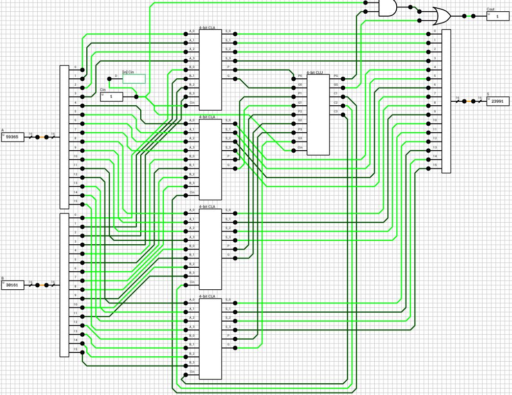
The 16-bit CLA is shown in figure 4. It uses 4 instances of the 4-bit CLA component from figure 2 and 1 instance of the same Carry Lookahead Unit (CLU) used in the 4-bit CLA circuit. The CLU takes the 4 (P,G) pairs generated by the 4-bit CLAs, as well as the Cin input, and calculates PG and GG. From those two the final carry output is calculated, using the same subcircuit as in the 4-bit CLAs (Cout = GG + PG*Cin).
The total gates required for this circuit is: 32XOR + 85AND2 + 67AND4 + 51AND3 + 34OR4 + 17OR3 + 18OR2. The worst case delay is 12T, including the 2T overhead of the mergers/splitters.
Figure 4: 16-bit CLA
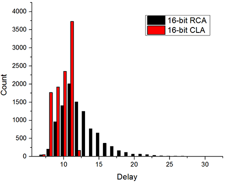
Comparison
From the above it’s clear that the CLA is a lot faster than the RCA, but it requires many more gates. Looking at the maximum delays when comparing the 2 circuits might not tell the whole truth though. Figure 5 shows a histogram from 10k random changes to the inputs of both circuits. The X axis is the measured circuit delay and the Y axis is the number of occurrences. The worst case delay for the RCA might be 32T but the average is a lot less. The most frequent delays is around 11T for both circuits.
Figure 5: Comparison between the 2 circuits
That’s all for now. Thanks for reading. Comments and corrections
are welcome.
The past few days, I’ve added a basic logic analyzer in DLS (not yet released; will be available on v0.10). You can add probes in the schematic and connect them to output pins, in order to observe the timing of the signals coming out of them.
Having a way to observe signals as they pass through the circuit, instead of just observing their steady state at the end of the simulation, can help you find glitches or compare the speed of 2 different versions of the same circuit.
I decided to test it out by implementing 2 different versions of a 4-bit adder. One would be a ripple-carry adder and the other would be a carry lookahead adder. Ideally, the latter should be faster than the former (i.e. the sum and output carry should be available quicker), so let’s see if this is actually true in DLS.
But first some words about DLS, in case you haven’t heard about it before.
A few words about DLS
It’s been almost 9 months since I uploaded v0.1 of DLS on
itch.io. DLS is an event-driven unit-delay 4-value digital logic simulator.
Event driven means that a component/gate is simulated only if one of its inputs change value.
Unit-delay means that all basic gates (AND,OR,etc.) have the same propagation delay, which is assumed to be 1 (in arbitrary time units).
4-value logic means that signals can be in one of 4 states, 0, 1, Undefined and Error. Undefined means either that the signal can be either 0 or 1 (e.g. AND(U,1) = U, AND(U,0) = 0), or that it’s in high impendance state (e.g. when used as input to a bus). Error is produced only by tristate buffers when the control signal is Undefined.
One of the reasons I started working on it was because
apparently I suck at VHDL and I wanted an easier way to play around with logic circuits. The other reason was that I like simulations of any kind, so what’s a better way to learn how digital circuits work than writing a simulator :)
Fast forward 9 months, DLS can successfully simulate semi-complex circuits, built with either
basic logic gates or
scripts. There are probably a lot of things wrong in those circuits, but since they seem to work, who am I to complain :)
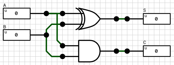
1-bit Half Adder
Let’s start small. A 1-bit half adder is shown in figure 1. It adds 2 1-bit binary inputs (A and B) and produces 2 1-bit outputs. One for the Sum (S) and one for the Carry (C). For more info see the
wikipedia article on adders.
Figure 1: 1-bit half adder
Taking into account that both the XOR and the AND gate is assumed to have the same propagation delay, we would expect both outputs (S and C) to settle at their final value after 1T (1T = 1 gate delay). Figure 2 confirms that.
Figure 2: 1-bit half adder timing graph
1-bit Full Adder
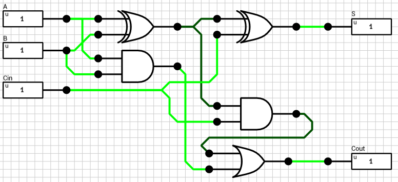
Half adders aren’t that useful though. In order to add 2 (e.g.) 2-bit binary numbers you have to take into account the carry out of the LSB addition when calculating the sum of the MSB. A 1-bit full adder does that. In addition to the A and B inputs, it has a 3rd 1-bit input which is the carry of the previous, less significant, stage. Figure 3 shows the circuit of a 1-bit full adder.
Figure 3: 1-bit full adder
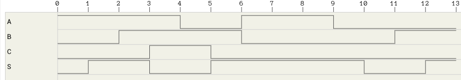
From the above schematic it’s obvious that the maximum time required for a stable signal at the S output is 2T, when one of A or B switches value (but not the other), which forces the first XOR gate to change value.
The maximum time for the Cout output is 3T, because the AND gate in the Carry part of the circuit (lower right) has to wait 1T until the value of the first XOR is computed. E.g. B=0, A=0->1 and Cin=0->1.
Figure 4 shows the timing graph from various changes to the inputs of the full adder.
Figure 4: 1-bit full adder timing graph
There’s one glitch in this circuit. For A = Cin = 1 and B = 1->0, Cout changes value twice. This is because the first AND gate changes value at T=1 which forces the OR gate to switch at T=2. But at T=2 the second AND gate changes value which in turn makes the OR gate to switch again at T=3.
Is it possible to fix that glitch and keep the same latency? Probably not, but we should keep that in mind in case we want to use Cout as the clock input in a sequential circuit.
A note about critical paths
Finding the critical path of circuits like those presented above might be relatively easy to be done by hand. As circuits gets more complicated, finding the critical path is a very tedious process. To be honest I haven’t researched the subject until I started writing this article, so I can’t comment on any methods used in professional simulators.
Instead of trying to implement an existing algorithm to calculate the critical path of the circuits in this article, I used a testbench (you can write testbenches in DLS using Lua by the way :)). The testbench iterates 1000 times giving random values to all circuit inputs, and simulating the circuit once in each iteration. The current simulation time is read in every iteration, and the maximum dT is calculated. The input changes that produced the maximum dT give us the critical path of the circuit.
With that out of the way, lets move on.
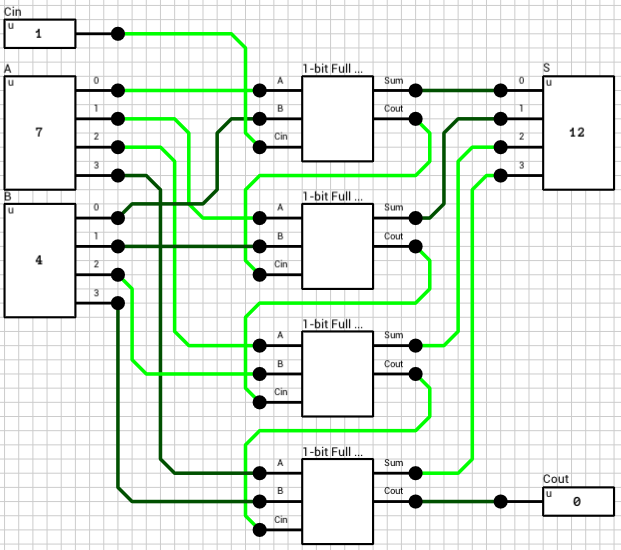
4-bit Ripple Carry Adder
The easiest way to build wider adders is to connect multiple 1-bit full adders in series. After all, this is the way we add two numbers on paper, isn’t it? The carry output of the i-th adder is used as the carry in to the (i+1)-th adder. The Cout of the last adder is the carry produced by the N-bit addition. This kind of adder is called a ripple carry adder.
Figure 5 shows a 4-bit ripple carry adder, which uses 4 instances of the 1-bit full adder component shown above.
Figure 5: 4-bit ripple carry adder
Sidenote: The circuit in fig. 5 has 2 4-bit inputs, A and B. In order to get the individual bit values from these 2 inputs we have to use a Wire splitter. In reality, there’s no such thing as a 4-bit wire, so there’s no need for such component. In DLS though, in order to be able to create manageable components (with as few I/O pins as possible), we have to use “fat” wires with splitters and mergers. Because DLS is a unit-delay simulator, those components must have a delay of at least 1T in order to work correctly. This might affect the timing of the circuit but since the same parts will be used later for the lookahead carry adder, it shouldn’t affect the comparison. The same is true for the 4-bit S output which requires a wire merger.
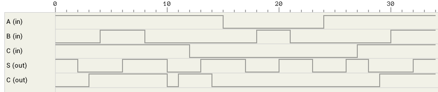
In figure 6 the timing for various changes to the inputs of the above circuit is shown. The maximum latency of this circuit is 10T. One of the configurations which require that amount of time to compute is show in the figure (A=13->10, B=5 and Cin=1).
Figure 6: 4-bit ripple carry adder timing graph
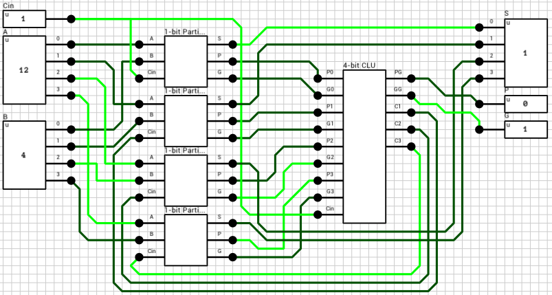
4-bit Carry-Lookahead Adder
Analyzing the theory behind Carry-lookahead Adders is beyong the scope of this article. For details on them you can check the corresponding
wikipedia article.
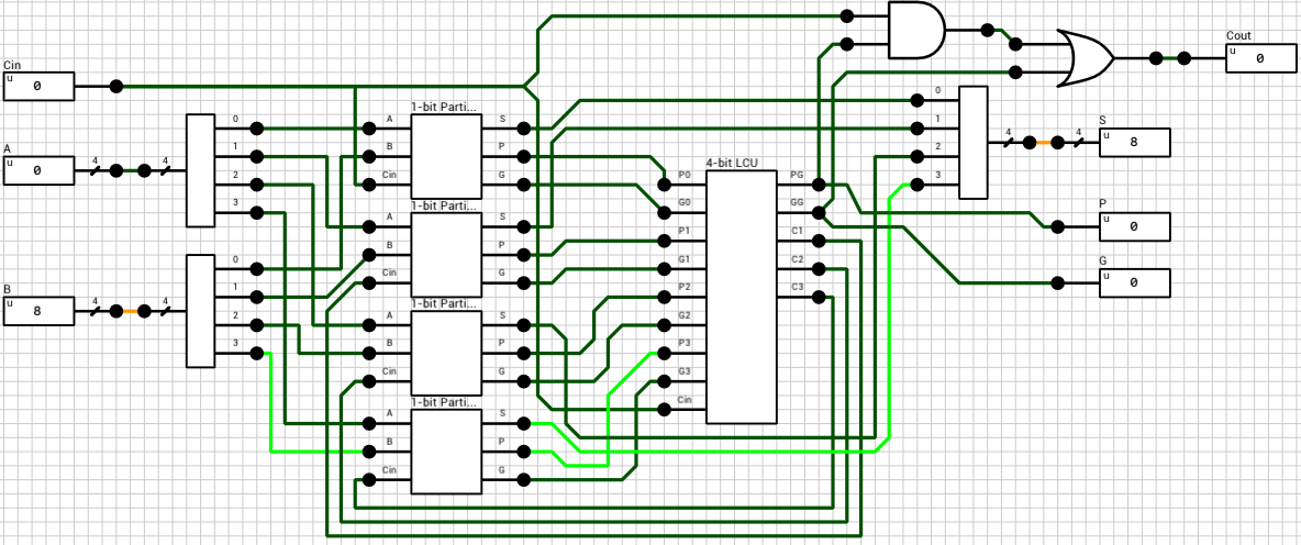
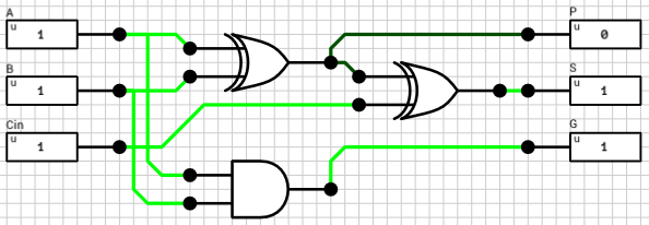
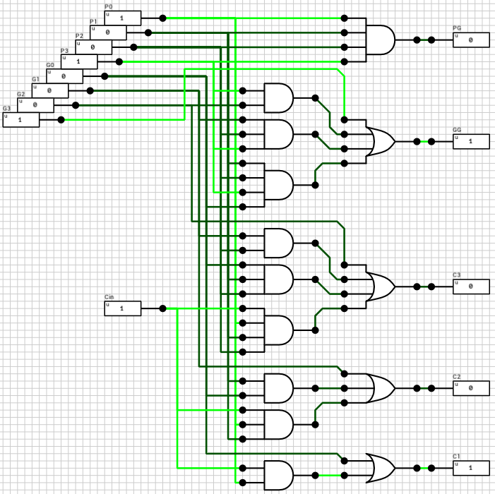
Figure 7 shows the circuit of a 4-bit Carry-lookahead adder. The 4 1-bit Full adders have been replaced by 1-bit Partial adders (figure 8) and a Lookahead Carry Unit (LCU) (figure 9) has been added. The LCU’s function is to calculate PG and GG which is used for the final carry output, as well as the carries which will be used as inputs for the last 3 partial adders.
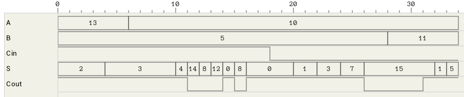
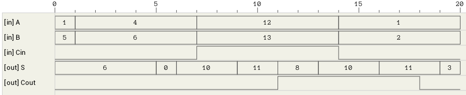
The maximum latency of this circuit is 6T, with the critical path being from the inputs to S (Cout has been calculated 2T earlier). Figure 10 shows one of the worst cases (A=4->12, B=6->13, Cin=0->1).
Apparently Carry-lookahead adders are actually faster than Ripple-carry adders, even in DLS! The extra latency introduced by the wire splitters and mergers is present in both versions, so it shouldn’t affect the comparison.
Next time, I’ll try expanding both adders to 16 bits to see if the difference gets even larger (it should). The problem with 16 bits, in case we want to reuse both of the above circuits as components, is that it requires splitting 2 16-bit wires and merging them into 4-bit groups, which will in turn be connected to the individual 4-bit adders. This alone adds a latency of 3T + 3T (3T for splitting inputs + 3T for merging outputs), but again the comparison should be fair if we apply the same methodology to both versions (I suspect that even if we cheat a bit in favor of the ripple carry adder, the CLA will still be faster overall).
Thank you for reading.
Hope to be able to write more about circuits and DLS in the following weeks/months. So if you find any mistakes or have any comments on what I wrote, I’d appreciate
you feedback.