Having implemented an adder, the next step is… to use it in a larger circuit :) Today I’ll try to describe the process of creating a simple Arithmetic/Logic Unit (ALU) in DLS, using the 16-bit CLA from the last post.
ALUs typically support several different functions, instead of just additions, and also output several extra flags to describe the result of the selected function (I think that’s the reason Logic is in the title). The ALU I’ll present will also support 4 bitwise operations and subtraction. Multiplication, division and arithmetic/logical shifting will (probably) be discussed in a future article, as I don’t think they are necessarily a good fit for an ALU (e.g. multiplication can be performed algorithmically in mutliple cycles using repeated additions and shifting might be needed outside the ALU in order to support shifting its result in the same cycle).
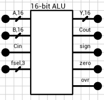
Figure 1 shows the final ALU as a component. It has 4 inputs and produces 5 outputs. Inputs A, B and Cin should be familiar from last time. fsel is used to select the function we want to execute on the other inputs. Table 1 shows the 7 supported functions and their corresponding fsel value. Note that there’s a spare slot (fsel = 7). This can be used later to expand the ALU with one extra function, but we must also take care to produce predictable results in case fsel is set to 7 by the user.
| fsel | Description |
|---|---|
| 0 | NOT(A) |
| 1 | AND(A, B) |
| 2 | OR(A, B) |
| 3 | XOR(A, B) |
| 4 | A + B + Cin |
| 5 | A - B - Cin |
| 6 | B - A - Cin |
Table 1: ALU’s function table
The component’s outputs are:
Y: the 16-bit result of the selected functionCout: the output carry of the selected function (if any)zero: when HIGH it means thatYis zerosign: the most significant bit ofYovr: when HIGH it means that an overflow has occured andYis invalid. It can happen when (e.g.) the addition of 2 positive numbers produces a negative result.
Output buses and fsel decoder
The way the ALU will be implemented is by calculating all the supported functions in parallel and have a bus at the end which will select the correct output based on the current value of fsel. Figure 2 shows the Y bus. There are 7 different results calculated and each one of them is connected to a 16-bit tristate buffer. All tristate-buffers are then connected to a 8x16-bit bus.
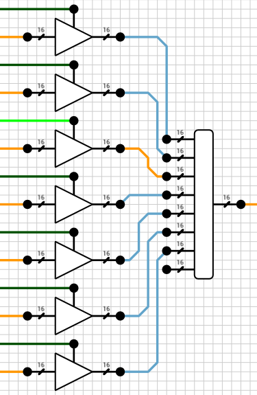
Despite the fact that there are only 7 functions, because fsel is 3 bits wide I used a 8x16-bit bus instead of a 7x16-bit bus, to be able to expand the ALU later. Note that the last bus input isn’t connected to anything and will, by default, have an Undefined value. So, for fsel = 7, Y = Undefined.
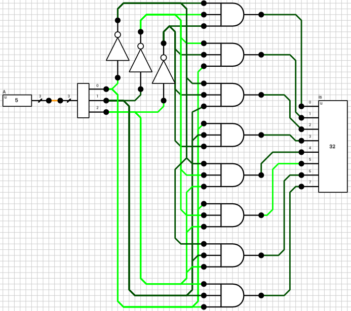
In order to control the 7 tristate buffers, we first need to decode fsel. A 3-to-8 decoder does the job (figure 3). It has only one input (a 3-bit value) and 8 1-bit outputs. When the i-th output is HIGH, it means that the input number is i. Only one of the outputs can and will be HIGH for any given input value.
Bitwise operations
The first 4 functions are easy to implement, especially in the latest version of DLS which supports multi-bit standard gates. Figure 4 shows the subcircuit used to calculate those functions.
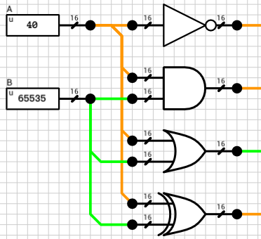
Only a single multi-bit gate is needed for each case. The outputs are routed to their respective tristate buffers we saw earlier. None of these functions make use of the Cin input, so it’s ignored.
Addition/Subtraction
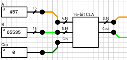
The 5th function is the addition of the two inputs taking into account Cin (Y = A + B + Cin). Using the 16-bit CLA adder we created in the previous article, we can easily calculate both Y and Cout for this case (figure 5).
Calculating the difference of 2 two’s complement binary numbers A and B can be done using the same 16-bit CLA. If we take into account that A - B = A + (-B) and -B = NOT(B) + 1, where NOT(B) is the one’s complement of B, Y = A - B ends up being translated to Y = A + NOT(B) + 1.
This means that in order to use the CLA for subtraction it is required to invert B and Cin. Cin needs to be inverted because A - B - 1 = A + NOT(B) + 1 - 1 = A + NOT(B). Finally for fsel = 6 we need to swap A and B before doing any of that. Table 2 shows the 3 different cases.
| fsel | CLA.A | CLA.B | CLA.Cin | Y |
|---|---|---|---|---|
| 4 | A | B | Cin | A + B + Cin |
| 5 | A | NOT(B) | NOT(Cin) | A - B - Cin |
| 6 | B | NOT(A) | NOT(Cin) | B - A - Cin |
Table 2: CLA inputs and expected result for functions 4, 5 and 6
There are 2 ways to implement the subcircuit which will control the CLA inputs. Either use three 4-input multiplexers (MUX), one for each CLA input, with an invalid/duplicate sel code, or break the decision tree into 2 steps and use only 2-input MUXes (which avoids having invalid/duplicate sel codes). I’ll describe the second method.
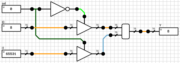
The first step is to decide if we need to swap A and B. This is done by using two 16-bit 2-input multiplexers (figure 6), with their sel input connected to the 7-th output pin of the fsel decoder (because only function 6 needs reversed inputs). The 1st MUX has I0 = A and I1 = B. The 2nd MUX has I0 = B and I1 = A. When fsel = 6, the 7-th output pin of the decoder will be HIGH and both MUXes will select their I1 inputs (B and A respectively). In all other cases, both MUXes will select their I0 inputs (A and B respectively)
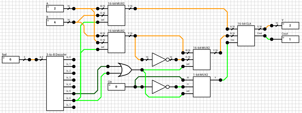
The second step is to check if we need to invert B and Cin. This is done by ORing the 6th and 7th output pins of the fsel decoder (meaning that the operation is a subtraction) and using the result as input to 2 multiplexers; a 16-bit one for the second operand and a 1-bit for Cin. Finally the multiplexer outputs are connected to the CLA. Figure 7 shows the relevant subcircuit.
Cout
Up to this point I’ve only talked about the Y output, because this was the most complicated of them. The 2nd output is Cout. For fsel = 0,1,2,3, Cout will always be 0, because the operations do not produce a carry. For fsel = 4,5,6, Cout is the carry output of the CLA. Using 1-bit tristate buffers and a 8x1-bit bus, as with Y, will do the trick. Figure 8 shows the relevant subcircuit.
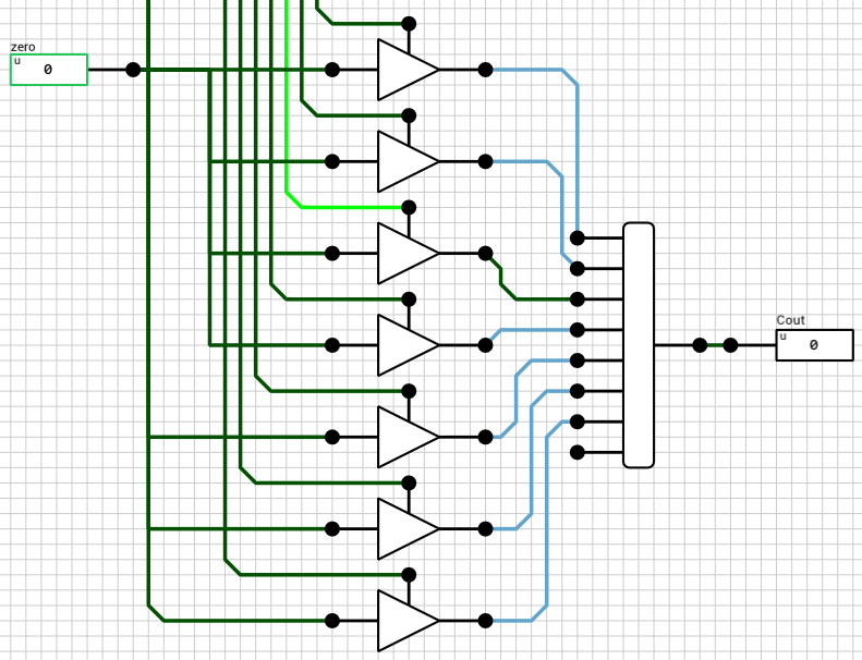
NOTE: Input ports with a green border, such as the zero port in the above figure, are constants. This means that when the circuit is turned into a component, those ports will not appear as inputs pins on the component.
Flags
The last thing we have to implement is the calculation of the 3 flags I mentioned above, zero, sign and ovr.
zero can be calculated by NORing all the bits of the Y output. In DLS this requires using a wire splitter to get the individual bits of the wire and a 16-input 1-bit NOR gate. If any of the bits of Y is HIGH, Y is not zero and NOR will return LOW. If all the bits of Y are LOW NOR will return HIGH.
sign is the MSB of Y. Since we already used a wire splitter to calculate the zero flag, we can grab the 16-th pin and connect it to the sign output port.
ovr is a bit more complicated. Overflow can only happen when, adding two numbers with the same sign produces a result with a different sign (
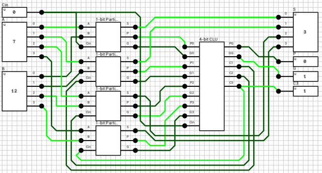
reference). In our case we should also take into account the input carry. The easiest way to see if overflow has occurred is inside the adder. By comparing the carry into the sign bit with the carry out of the adder we can detect overflow. In order to implement this method, we have to revisit the CLA and make a small adjustment. Figure 9 shows the new 4-bit CLA. The carry into the sign bit is the C3 output of the 4-bit CLU.
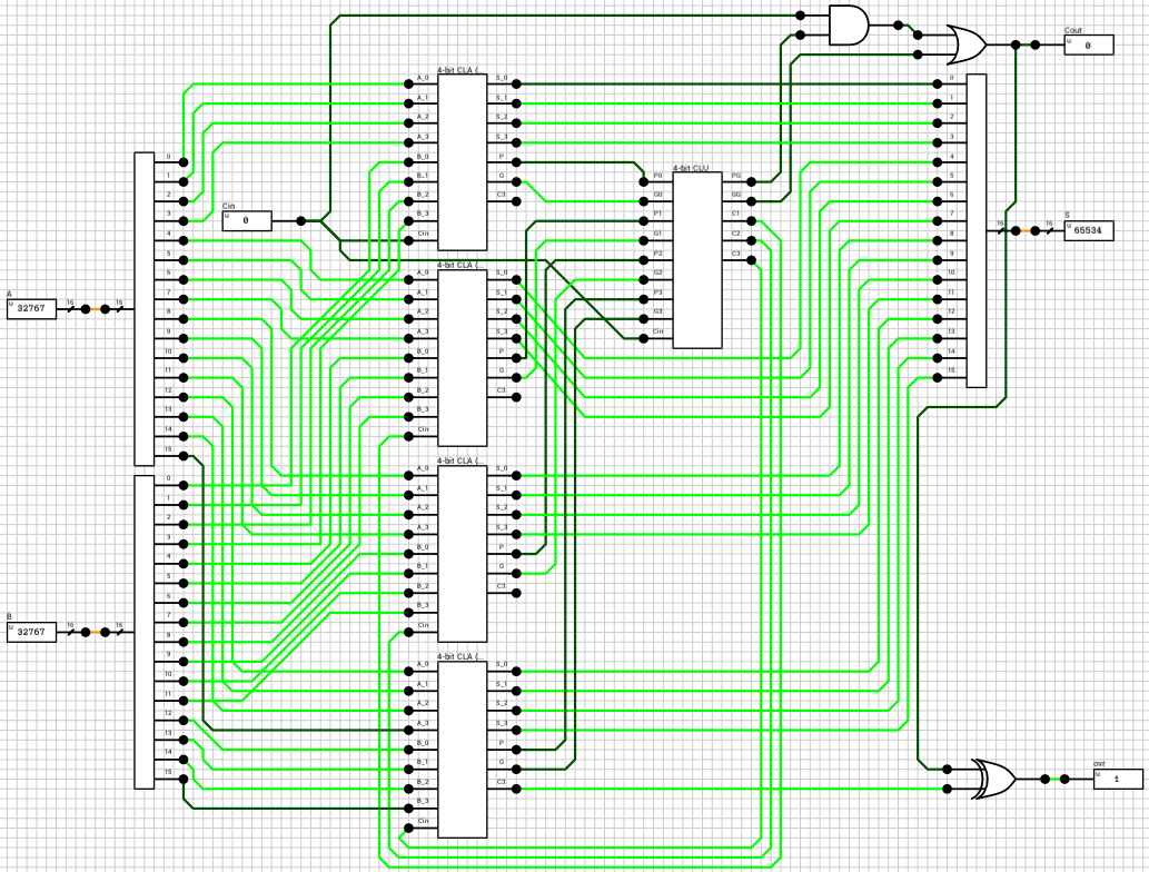
After replacing the four 4-bit CLAs in the 16-bit CLA circuit with the new components, the ovr flag is calculated by XORing the C3 output of the last 4-bit CLA with the final carry out of the adder (figure 10).
Complete circuit
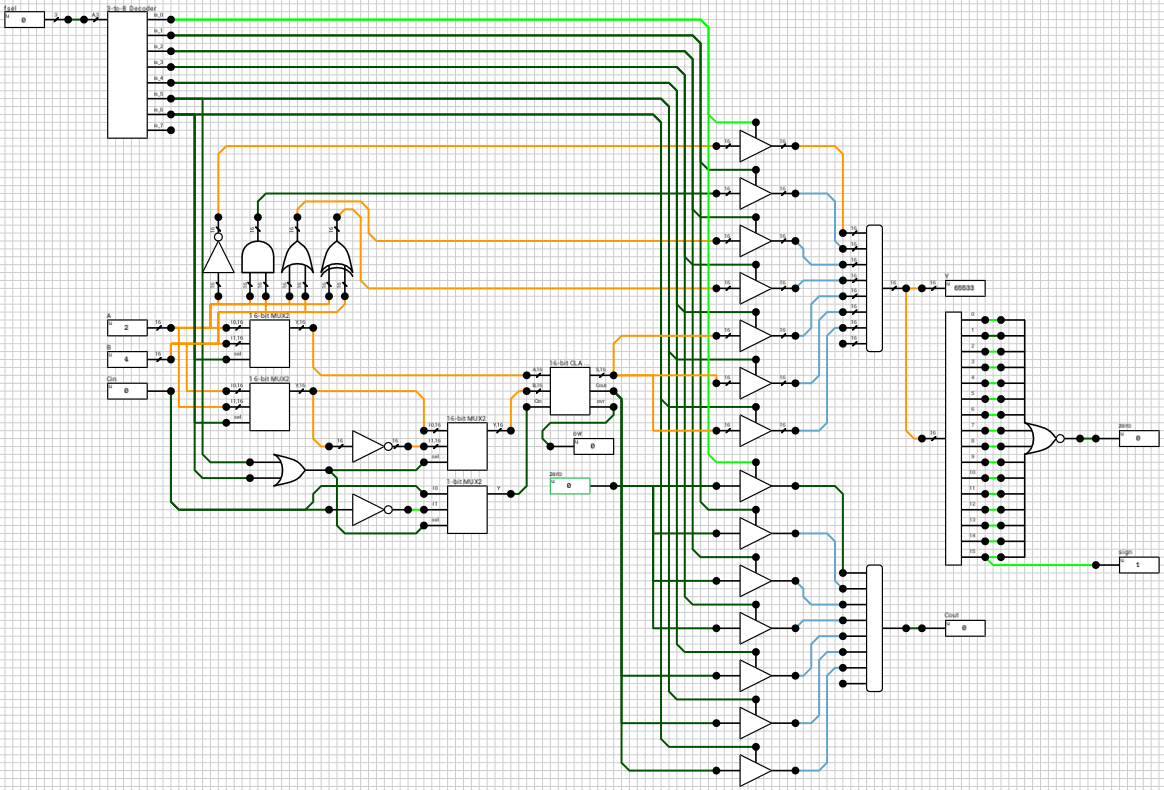
Figure 11 shows the final circuit. I haven’t measured the delay of the various functions, and I suspect there might be a couple of changes which might help in this area, but since the article is getting really long, it’ll do for now. Knowing the worst case delay of the ALU might be needed in cases where correct timing of the results is required.
Thanks for reading. Comments and corrections are welcome.
PS. If you find it hard to read the schematics due to the large amount of wires, remember that wires meeting at a T junction are connected, and wires crossing each other are not connected. Hope it helps :)