If you happen to be one of the two readers of this blog who have actually checked out the circuits I’ve posted, you might have found out that the register file circuit (RF) I presented in an
earlier post doesn’t work quite right. If you tried it out by manually changing the input values (e.g. rD and dD), everything appears to work correctly. Whenever the clock ticks, the new value is written to the selected register.
The problem I’m going to talk about appears when you try to use this component as part of a larger circuit. If you connect your clock directly to the clk input of the RF but the dD and rD inputs are connected to some other component’s output, you’ll need 2 clock ticks to actually write the new value to the selected register. This is because I didn’t pay attention to propagation delays when designing the various components and the clock signal arrives to the flip flops before the new data signal.
So, let’s fix the circuit by starting from the basic element of the RF, as I did in the original post.
Positive edge triggered D flip flop
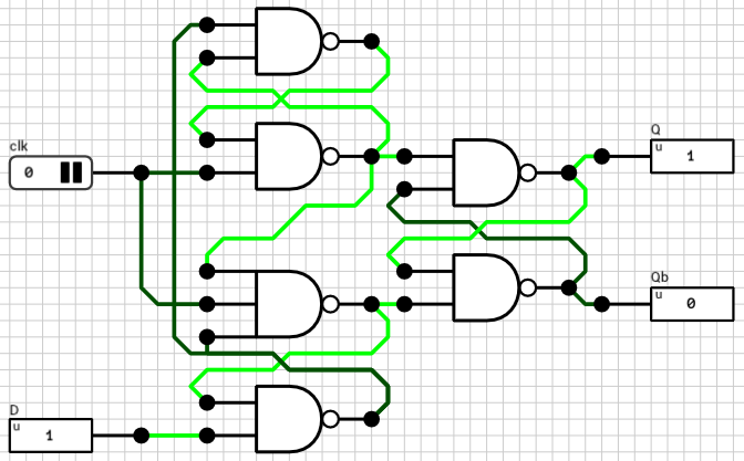
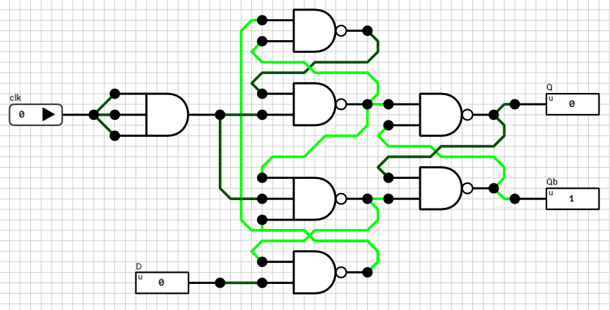
The original DFF I used is shown in figure 1 for reference. Ideally, whenever clk goes from LOW to HIGH, the current D value is reflected on the Q output. Unfortunately, this isn’t true. In order to test it out we need a testbench. Since D is an 1-bit signal, there are two transitions to consider: D going from LOW to HIGH and vice versa.

There are 3 different cases when it comes to the timings of clk and D inputs.
clksignal arrives beforeDclksignal arrives at the same time asDclksignal arrives afterD
Cases 2 and 3 are the ones we are interested in. The 1st case works correctly because if the clock signal arrives before the new data, it means that the controlling circuit wanted to write the old data to the flip flop. In other words, it’s the controlling circuit’s responsibility to synchronize the two signals.
On the other hand, if the rising edge of clk arrives after the new D value, we must assume that the new data will be written to the flip flop. So, the worst case scenario is that both clk and D arrive at the exact same time.
In order to find out if the current circuit works as expected, I used a testbench. Testbenches are an easy way to change multiple input values at the same time before triggering a simulation. Script 1 below shows the testbench I used.
-- Reset the circuit to a known state
set("clk", 0);
set("D", 0);
simulate();

-- D 0 -> 1
set("D", 1);
tick("clk");
assert(get("Q") == 1, "Failed");
assert(get("Qb") == 0, "Unstable!");
tick("clk");

-- D 1 -> 0
set("D", 0);
tick("clk");
assert(get("Q") == 0, "Failed");
assert(get("Qb") == 1, "Unstable!");
tick("clk");
Script 1: DFF testbench
Initially the circuit is reset to a known state (clk = 0 and D = 0). The first test is for the LOW-to-HIGH D transition and the second and final test is for the HIGH-to-LOW transition. Remember that tick() toggles the specified clock value and triggers a simulation.
If you execute this testbench in the simulator you’ll find out that the HIGH-to-LOW transition of the D signal doesn’t work (the first assert of the second test is triggered and the testbench is terminated). This means that when D goes from HIGH to LOW, the time required for the clk signal to arrive to the output latch is less than the time required for the new D value, which results in the old D value being written to it.
In order to fix it, the clock signal should be delayed. The easiest way to delay a signal in the current version of DLS is to use an AND gate. By passing the same signal to all its inputs, you get the same value on its output, at a later (internal) timestep. In DLS, each basic gate has its own propagation delay, which is dependent on the number of inputs (check appendix A of the manual for details). In our case, an AND2 gate has a delay of 1T and an AND3 gate has a delay of 2T.
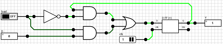
By trial and error, I found that the required delay for the clock signal is 2T (a single AND3 gate or two AND2 gates in series). The final, corrected, DFF circuit is shown in figure 2.
The testbench works correctly with this circuit. This means that if the controlling circuit sends both signals at the exact same timestep, the flip flop will work correctly. If the clock signal arrives at a later timestep than the D signal it will also, by definition, work correctly.
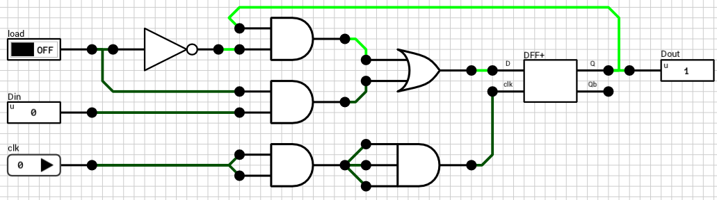
1-bit Register
In the same vein, let’s test the original 1-bit register (figure 3). In this case, there’s an extra 1-bit input (load) which determines if the new D value will be written to the flip flop or not. The testbench used to check this circuit is shown in Script 2.

-- Reset circuit
set("clk", 0);
set("load", 1);
set("Din", 0);
simulate();

-- D: 0 -> 1, load: 1
set("Din", 1);
tick("clk");
assert(get("Dout") == 1, "Failed");
tick("clk");

-- D: 1 -> 0, load: 1
set("Din", 0);
tick("clk");
assert(get("Dout") == 0, "Failed");
tick("clk");

-- D: 0 -> 1, load: 1 -> 0
set("load", 0);
set("Din", 1);
tick("clk");
assert(get("Dout") == 0, "Failed");
tick("clk");

-- D: 1, load: 0 -> 1
set("load", 1);
tick("clk");
assert(get("Dout") == 1, "Failed");
tick("clk");

-- D: 1 ->, load: 1 -> 0
set("Din", 0);
set("load", 0);
tick("clk");
assert(get("Dout") == 1, "Failed");
tick("clk");
Script 2: 1-bit Register testbench
The delay of the critical path of the DFF controlling circuit (i.e. the multiplexer in front of the DFF) is 3T (from load to OR output). So in order to make D and clk arrive at the same time to the DFF component, the clock should be delayed by 3T (one AND2 gate and one AND3 gate in series). Figure 4 shows the new 1-bit register circuit which passes all the tests in the testbench.
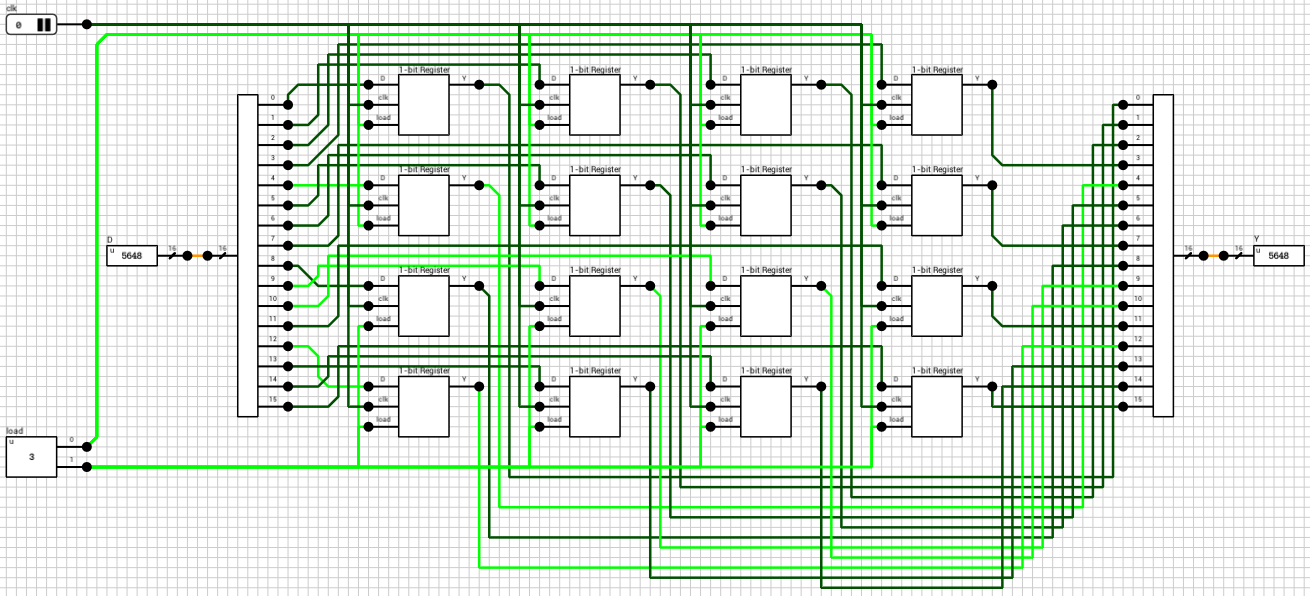
16-bit Register
Once more, the clock in the 16-bit register circuit should be delayed until the D signal is ready to be fed to the 1-bit registers. Only a 16-bit wire splitter exists between Din and the 16 1-bit registers and the wire splitter has a delay of 1T (independent of the number of bits). So by delaying the clock signal by 1T, both Din and clk arrive at the 1-bit registers at the same time. Note that the load signal is already split and directly connected to the registers, so it should be valid when clk and Din arrive.
Script 3 below shows the testbench for the final 16-bit register circuit from figure 5. This time, since the number of possible transistions of the Din signal are way too many to exhaust, I used random inputs for the Din port.
set("clk", 0);
set("Din", 0);
set("load", 3);
simulate();

local D = randBits(16);
set("Din", D);
tick("clk");
assert(get("Dout") == D, "Failed");
tick("clk");

for i=1, 1000 do
  local v = randBits(16);
  local load = randBits(2);

  set("Din", v);
  set("load", load);

  tick("clk");

  local expectedValue = v;
  if(load == 0) then
    expectedValue = D;
  elseif(load == 1) then
    local low = bit.band(v, 0x00FF);
    local high = bit.band(D, 0xFF00);
    expectedValue = bit.bor(low, high);
  elseif(load == 2) then
    local low = bit.band(D, 0x00FF);
    local high = bit.band(v, 0xFF00);
    expectedValue = bit.bor(low, high);
  else
    expectedValue = v;
  end

  assert(get("Dout") == expectedValue, "Failed");

  D = expectedValue;

  tick("clk");
end
Script 3: 16-bit Register testbench

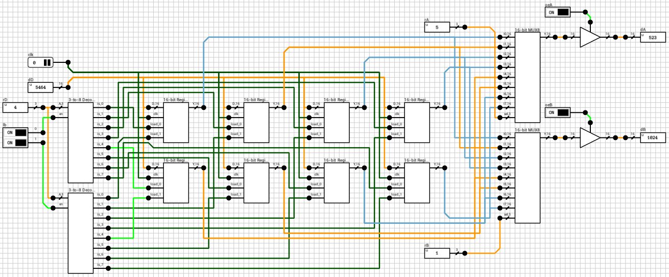
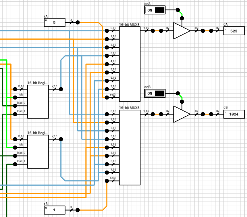
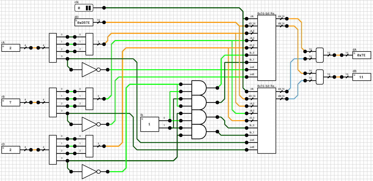
8x16-bit Register file
Finally it’s time to look the actual register file circuit (figure 6). We are only interested in the write part of the circuit, since reading is performed asynchronously (whenever rA, rB, oeA or oeB change, the outputs are immediately updated, without waiting for a clk rising edge).
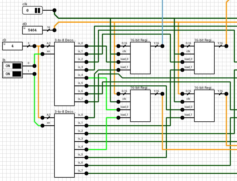
Both dD and clk are directly connected to the corresponding inputs of all 8 registers so it’s probably expected that the circuit will work correctly once we replace the old registers with the new components presented above. Script 4 shows a small testbench.
-- Reset the circuit. Don't touch dD for extra randomness :)
set("rA", 0);
set("rB", 1);
set("rD", 0);
set("lb", 3); -- Write both bytes to simplify testing
set("clk", 0);
simulate();

-- Test 1: Write a random value to register 0.
local v = randBits(16);
set("dD", v);
tick("clk");
assert(get("dA") == v, "Failed");
tick("clk");

-- Test 2: Write a random value to register 1.
local v2 = randBits(16);
set("dD", v2);
set("rD", 1);
tick("clk");
assert(get("dA") == v, "Failed");
assert(get("dB") == v2, "Failed");
tick("clk");
Script 4: 8x16-bit Register File testbench
As always, the circuit is first reset to a known state. rA and rB are pointed to registers 0 and 1 respectively, rD (the destination register) is set to 0 and lb is set to 3, meaning both bytes will be written, to simplify testing.
Test 1 tries to write a new random value to register 0. What’s expected is that when clk rises, the new value should be written to the register and dA should be updated to reflect it. This works correctly, since the registers have been corrected to handle both signals arriving at the same time.
The 2nd test tries to write another random value to register 1, by switching rD to 1 and dD to the new value, at the same timestep. It’s expected that when clk rises, the new value should be written to the register and dB should be updated to reflect it. Unfortunately, this part doesn’t work correctly!
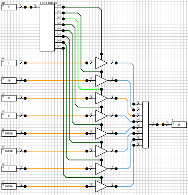
The reason is that there’s a delay on the load inputs of each register. By the time clk and dD arrive at the registers, the old rD is used to select the destination, because the 3-to-8 decoder haven’t had a chance to calculate its new output yet.
Looking at the 3-to-8 decoder (figure 7), the critical path delay is 4T, from A to is (1T for the wire splitter, 1T for the NOT gates and 2T for the AND4 gates). So, delaying the clk signal by 4T should do the trick.
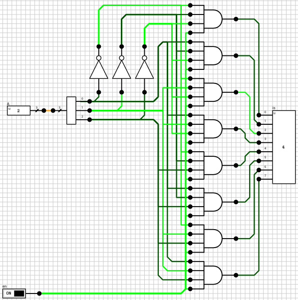
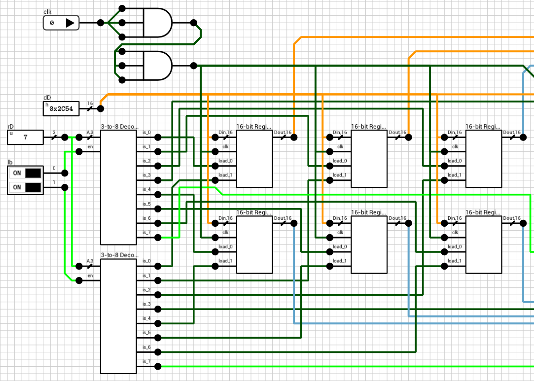
Figure 8 shows the final register file circuit. The 4T delay has been added to the clk signal using two AND3 gates.
Conclusion
If there’s something to keep in mind from this post is that whenever there’s a register/flip flop in a circuit, you should make sure that clock’s rising or falling edge arrives to it at the same time or after the data signal. Otherwise, you might need an extra clock cycle to actually store the new value in the register.
Note that the old version worked correctly in all other aspects. It just needed an extra rising edge to actually write the new value to the registers, which sometimes might be annoying when trying to debug it. Having the register file behave in the way we did in this post will make things a bit easier to debug when this component is used in a larger circuit.
Until the next post, comments/suggestions/corrections are welcome.