The past few days, I’ve added a basic logic analyzer in DLS (not yet released; will be available on v0.10). You can add probes in the schematic and connect them to output pins, in order to observe the timing of the signals coming out of them.
Having a way to observe signals as they pass through the circuit, instead of just observing their steady state at the end of the simulation, can help you find glitches or compare the speed of 2 different versions of the same circuit.
I decided to test it out by implementing 2 different versions of a 4-bit adder. One would be a ripple-carry adder and the other would be a carry lookahead adder. Ideally, the latter should be faster than the former (i.e. the sum and output carry should be available quicker), so let’s see if this is actually true in DLS.
But first some words about DLS, in case you haven’t heard about it before.
A few words about DLS
It’s been almost 9 months since I uploaded v0.1 of DLS on itch.io. DLS is an event-driven unit-delay 4-value digital logic simulator.
- Event driven means that a component/gate is simulated only if one of its inputs change value.
- Unit-delay means that all basic gates (AND,OR,etc.) have the same propagation delay, which is assumed to be 1 (in arbitrary time units).
- 4-value logic means that signals can be in one of 4 states, 0, 1, Undefined and Error. Undefined means either that the signal can be either 0 or 1 (e.g. AND(U,1) = U, AND(U,0) = 0), or that it’s in high impendance state (e.g. when used as input to a bus). Error is produced only by tristate buffers when the control signal is Undefined.
One of the reasons I started working on it was because apparently I suck at VHDL and I wanted an easier way to play around with logic circuits. The other reason was that I like simulations of any kind, so what’s a better way to learn how digital circuits work than writing a simulator :)
Fast forward 9 months, DLS can successfully simulate semi-complex circuits, built with either basic logic gates or scripts. There are probably a lot of things wrong in those circuits, but since they seem to work, who am I to complain :)
1-bit Half Adder
Let’s start small. A 1-bit half adder is shown in figure 1. It adds 2 1-bit binary inputs (A and B) and produces 2 1-bit outputs. One for the Sum (S) and one for the Carry (C). For more info see the wikipedia article on adders.
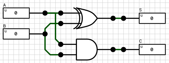
Taking into account that both the XOR and the AND gate is assumed to have the same propagation delay, we would expect both outputs (S and C) to settle at their final value after 1T (1T = 1 gate delay). Figure 2 confirms that.
1-bit Full Adder
Half adders aren’t that useful though. In order to add 2 (e.g.) 2-bit binary numbers you have to take into account the carry out of the LSB addition when calculating the sum of the MSB. A 1-bit full adder does that. In addition to the A and B inputs, it has a 3rd 1-bit input which is the carry of the previous, less significant, stage. Figure 3 shows the circuit of a 1-bit full adder.
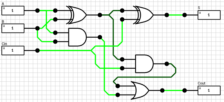
From the above schematic it’s obvious that the maximum time required for a stable signal at the S output is 2T, when one of A or B switches value (but not the other), which forces the first XOR gate to change value.
The maximum time for the Cout output is 3T, because the AND gate in the Carry part of the circuit (lower right) has to wait 1T until the value of the first XOR is computed. E.g. B=0, A=0->1 and Cin=0->1.
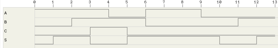
Figure 4 shows the timing graph from various changes to the inputs of the full adder.
There’s one glitch in this circuit. For A = Cin = 1 and B = 1->0, Cout changes value twice. This is because the first AND gate changes value at T=1 which forces the OR gate to switch at T=2. But at T=2 the second AND gate changes value which in turn makes the OR gate to switch again at T=3.
Is it possible to fix that glitch and keep the same latency? Probably not, but we should keep that in mind in case we want to use Cout as the clock input in a sequential circuit.
A note about critical paths
Finding the critical path of circuits like those presented above might be relatively easy to be done by hand. As circuits gets more complicated, finding the critical path is a very tedious process. To be honest I haven’t researched the subject until I started writing this article, so I can’t comment on any methods used in professional simulators.
Instead of trying to implement an existing algorithm to calculate the critical path of the circuits in this article, I used a testbench (you can write testbenches in DLS using Lua by the way :)). The testbench iterates 1000 times giving random values to all circuit inputs, and simulating the circuit once in each iteration. The current simulation time is read in every iteration, and the maximum dT is calculated. The input changes that produced the maximum dT give us the critical path of the circuit.
With that out of the way, lets move on.
4-bit Ripple Carry Adder
The easiest way to build wider adders is to connect multiple 1-bit full adders in series. After all, this is the way we add two numbers on paper, isn’t it? The carry output of the i-th adder is used as the carry in to the (i+1)-th adder. The Cout of the last adder is the carry produced by the N-bit addition. This kind of adder is called a ripple carry adder.
Figure 5 shows a 4-bit ripple carry adder, which uses 4 instances of the 1-bit full adder component shown above.
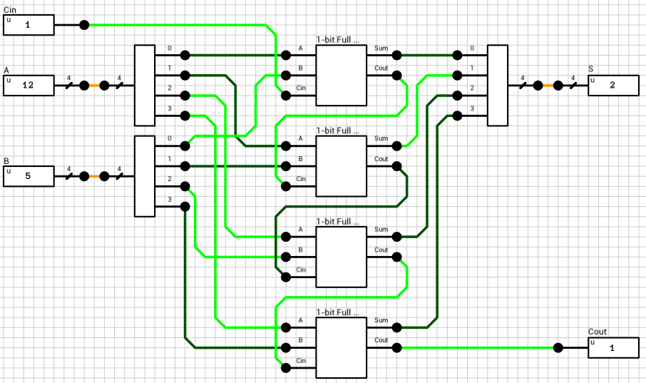
Sidenote: The circuit in fig. 5 has 2 4-bit inputs, A and B. In order to get the individual bit values from these 2 inputs we have to use a Wire splitter. In reality, there’s no such thing as a 4-bit wire, so there’s no need for such component. In DLS though, in order to be able to create manageable components (with as few I/O pins as possible), we have to use “fat” wires with splitters and mergers. Because DLS is a unit-delay simulator, those components must have a delay of at least 1T in order to work correctly. This might affect the timing of the circuit but since the same parts will be used later for the lookahead carry adder, it shouldn’t affect the comparison. The same is true for the 4-bit S output which requires a wire merger.
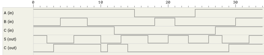
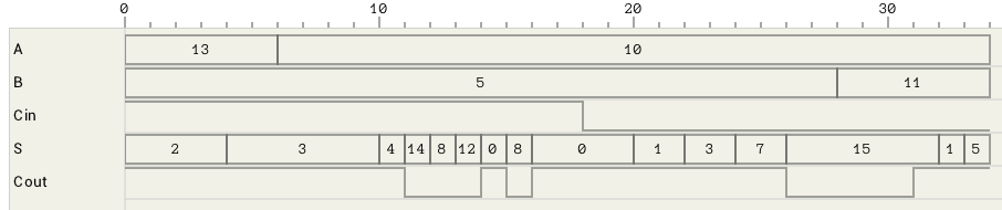
In figure 6 the timing for various changes to the inputs of the above circuit is shown. The maximum latency of this circuit is 10T. One of the configurations which require that amount of time to compute is show in the figure (A=13->10, B=5 and Cin=1).
4-bit Carry-Lookahead Adder
Analyzing the theory behind Carry-lookahead Adders is beyong the scope of this article. For details on them you can check the corresponding wikipedia article.
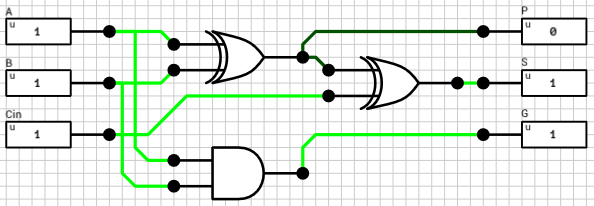
Figure 7 shows the circuit of a 4-bit Carry-lookahead adder. The 4 1-bit Full adders have been replaced by 1-bit Partial adders (figure 8) and a Lookahead Carry Unit (LCU) (figure 9) has been added. The LCU’s function is to calculate PG and GG which is used for the final carry output, as well as the carries which will be used as inputs for the last 3 partial adders.
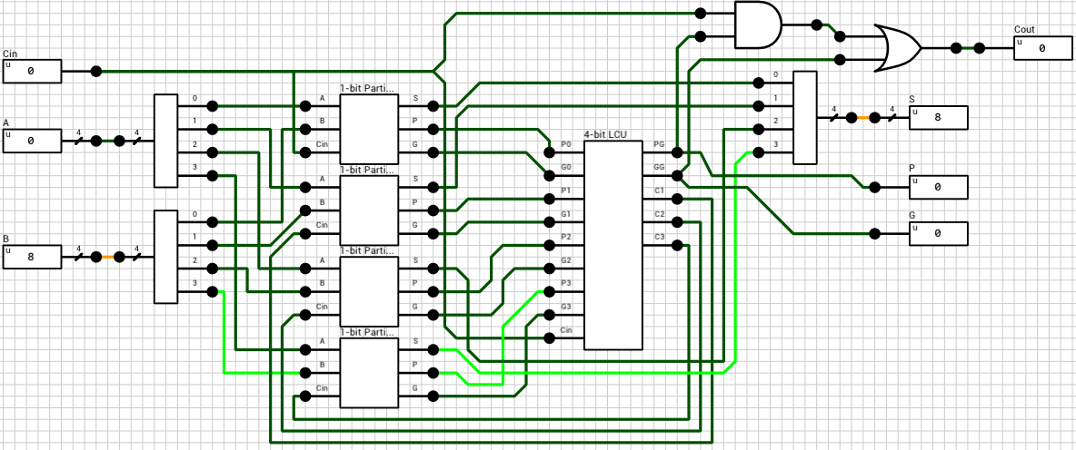
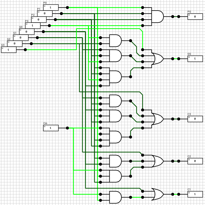
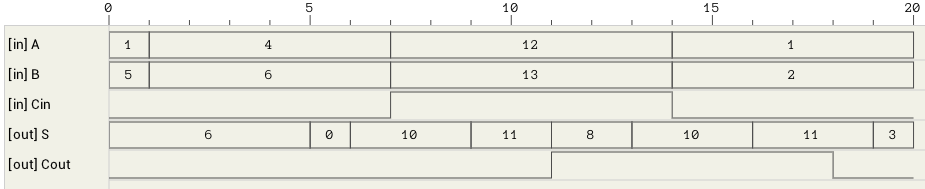
The maximum latency of this circuit is 6T, with the critical path being from the inputs to S (Cout has been calculated 2T earlier). Figure 10 shows one of the worst cases (A=4->12, B=6->13, Cin=0->1).
Closing
Apparently Carry-lookahead adders are actually faster than Ripple-carry adders, even in DLS! The extra latency introduced by the wire splitters and mergers is present in both versions, so it shouldn’t affect the comparison.
Next time, I’ll try expanding both adders to 16 bits to see if the difference gets even larger (it should). The problem with 16 bits, in case we want to reuse both of the above circuits as components, is that it requires splitting 2 16-bit wires and merging them into 4-bit groups, which will in turn be connected to the individual 4-bit adders. This alone adds a latency of 3T + 3T (3T for splitting inputs + 3T for merging outputs), but again the comparison should be fair if we apply the same methodology to both versions (I suspect that even if we cheat a bit in favor of the ripple carry adder, the CLA will still be faster overall).
Thank you for reading. Hope to be able to write more about circuits and DLS in the following weeks/months. So if you find any mistakes or have any comments on what I wrote, I’d appreciate you feedback.