The goal of today’s post is to build a 8x16-bit register file, i.e. a bunch of memory elements packaged as a single component. Figure 1 shows the final component we are going to build. It can read two registers asynchronously and write one of them on the rising edge of the supplied clock.

The first input is the clock (clk). The 16-bit value dD will be written to the register pointed by rD on the rising edge of the clk input. Since the registers will be 2 bytes wide, each byte can be independently written via the lb_0 and lb_1 inputs (lb = load byte).
Inputs rA and rB are the two registers we are interested in reading. Their current value will be available on the dA and dB outputs. Note that these 2 won’t be synchronized to the clk input. They can change at any moment and their respective output will be updated (almost) immediately.
Finally, oeA and oeB inputs (oe = output enable) control whether the corresponding output will hold the current value of the selected register, or if it will float. This way, we can use multiple instances of this register file to increase the number of available registers in a circuit, by combining all their outputs on a common bus. More on this at the end of the post.
Positive edge triggered D flip flop
Let’s start small. The basic building block for this component is the “Positive Edge Triggered D Flip Flop” shown in figure 2. It consists of three cross-coupled active LOW SR latches. Every time the clk input goes from LOW to HIGH, Q is updated to mirror the input D.
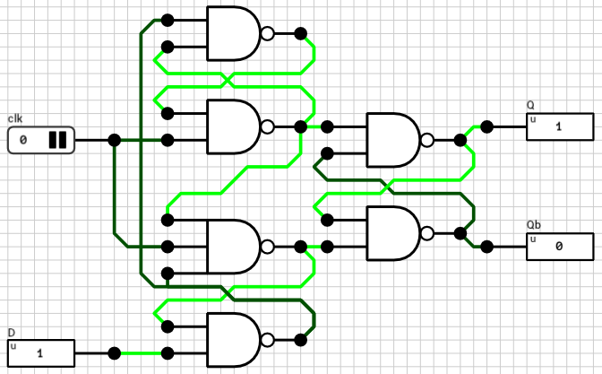
Qb is the complement of Q. It won’t be used later, but it’s there for completeness. The same flip flop can be used to build other kinds of circuits where Qb might be needed. The latches are connected in a way that the Q output is updated only on the transition of the clk input from LOW to HIGH (positive edge). In all other cases, no change on the D input will affect the Q output. For additional details take a look at the wikipedia article on
flip flops (paragraph “Classical positive-edge-triggered D flip-flop”).
1-bit Register
The flip flop from figure 2 can hold 1 bit of data. The clk input doesn’t need to be an actual clock. Any kind of 1-bit input can be used as a clock and it will be updated on its rising edge. In cases where the clk input is actually a free-running clock, we might have a problem if we don’t want to update its contents on the next rising edge. E.g. the wire connected to the D input changes value but we don’t want to store it in the flip flop on the next clock tick.
Figure 3 shows how this can be accomplished. By using a 2-input mutliplexer in front of the D input, with the first MUX choice being the old value and the second choice being the new value, we can select whether we want to update the flip flop or not, via the new load input.
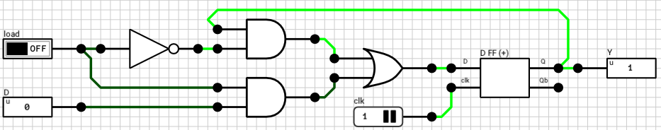
In order to distinguish this circuit from the flip flop shown above, I’ll call it an 1-bit Register.
Side note: I’ve created the mutliplexer using 2 AND and 1 OR gates instead of 2 tristate buffers and a 2x1-bit bus, as shown in the ALU post. This is because the tristate MUX has a small glitch which affects the rest of the circuit (at least in DLS). When changing the sel input of the tristate MUX, there’s a simulation timestep where both bus inputs are active at the same time. In such cases the buses in DLS are configured to output an Error value. If the output of the bus is connected to the D input of the flip flop, we might end up in an invalid state, from which it’s impossible to get out of. In the ALU circuit this wasn’t a problem since all components were combinational and they correctly handled Error inputs.
16-bit Register
Expanding to 16 bits is easy. We just use 16 instances of the 1-bit Register component, wire everything together and we are done. Figure 4 shows the 16-bit Register circuit.
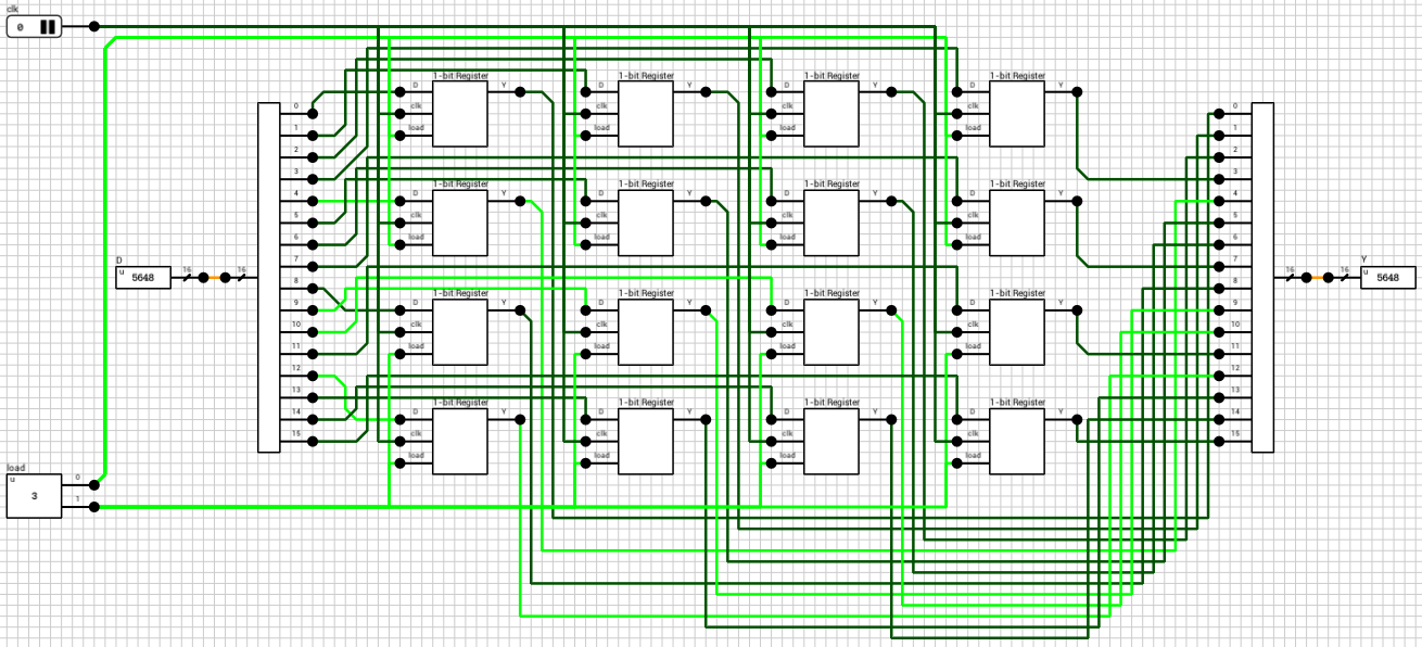
As I mentioned at the beginning of the post, since the register is 16 bits wide (2 bytes), we might want to control (write) each individual byte separately. This is the reason the load input is 2 bits wide. Each bit controls one of the bytes. If it’s not obvious from the figure, load_0 is connected to the load inputs of the first 8 1-bit registers and load_1 is connected to the load input of the other 8 1-bit registers.
Side note: The first time a register is initialized, both bytes should be written. The initial state of the D flip flop produces an Undefined output (because the clk hasn’t ticked yet). Since we don’t mask/split the register output to separate the individual bytes, having only 8 of the 16 bits initialized and the rest in an Undefined state will produce an Undefined value on the Y output. This is because, if at least 1 of the inputs on a wire merger is equal to Undefined or Error, the rest of the bits are ignored and the special state is propagated to the output.
The Register File
With the 16-bit Register component ready, we can now build a small register file. To keep things as simple as possible, we’ll use only 8 registers and (as mentioned in the intro) we’ll add a way to mask the outputs in order to be able to cascade multiple instances of this circuit to build larger files. Figure 5 shows the complete circuit. It might be a bit difficult to read, so I’ll break it up into parts, with zoomed in screenshots.
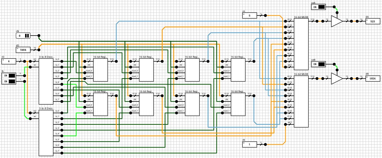
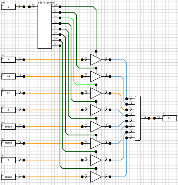
Figure 6 shows the write part of the circuit. clk is the clock and it’s routed to all the clk inputs of the 8 registers. dD is the 16-bit value we want to write to the rD register and it is again connected to the D inputs of all the registers. The 3-bit rD input is decoded using gated 3-to-8 decoders, one for each byte, based on the lb input. A gated decoder (figure 7) works the same way as the decoder we saw in the ALU post, with the only difference being that when its en input is LOW, all outputs are LOW.
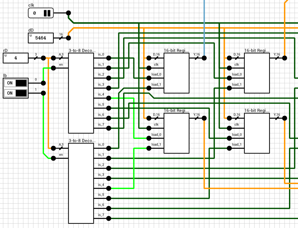
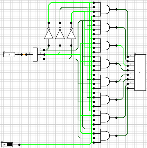
Figure 8 shows the read part of the circuit. All register outputs are routed to two 16-bit 8-input mutliplexers (figure 9). rA and rB are used as the sel input to the two MUXes. MUX outputs are connected to 16-bit tristate buffers, with the control pins connected to the oeA and oeB inputs.
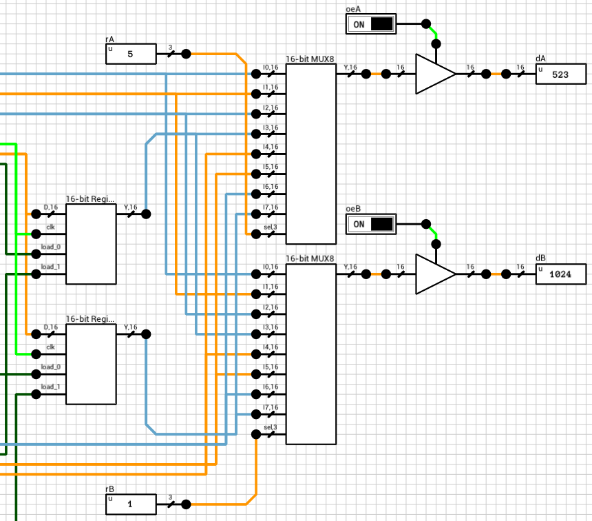
Note that in this case, since the MUX is after the flip flops, we can use tristate buffers. As long as the output of the register file isn’t connected to another register, there shouldn’t be a problem. If there is, we can always come back and replace the MUX with an AND/OR version.
Larger register files
The component presented above (figure 5) can be used to build both wider and deeper register files. Unfortunately, DLS doesn’t currently support bit widths larger than 16 bits per wire/pin, so building (e.g.) a 32-bit register file will end up in a mess of wires :) It’s possible, but you’ll need double the IO pins and wires.
Instead of building a wider file we’ll build a larger/deeper one, with 16 registers, using two instances of the component. In this case rA, rB and rD should be expanded to 4 bits, with their MSB used to select the correct file, by turning on or off the corresponding load and oe inputs. The dA and dB outputs of the two instances are connected on one bus each and then routed to the final outputs. Figure 10 shows the final 16x16-bit register file circuit.
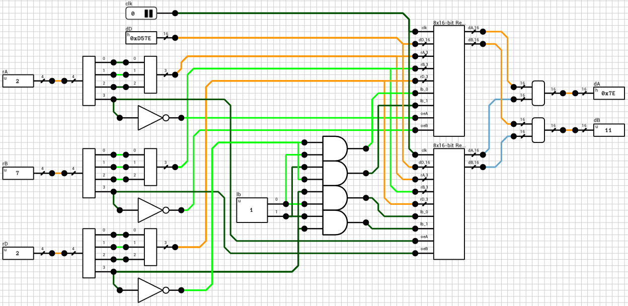
Note that in this circuit there’s no output enable inputs since I assumed this component won’t be used to build even larger components. If this is the case, both oe inputs should be exposed to correctly handle cascading.
That’s all for now. Thanks for reading. As always, comments and corrections are welcome.